

Confirmem-me, o topo de gama da AMD neste momento é o 9590, certo?

User Tag List
 Likes: 13
Resultados 91 a 105 de 1893
Tópico: AMD RyZen R7 / R5 / R3
-
30-06-15, 16:26 #91Master Business & GPU Man


- Registo
- Jan 2015
- Local
- País Campeão Euro 2016
- Posts
- 7,793
- Likes (Dados)
- 0
- Likes (Recebidos)
- 1
- Avaliação
- 41 (100%)
- Mentioned
- 0 Post(s)
- Tagged
- 0 Thread(s)
Ideias sem Nexo e Provas do Tráfico de Hardware
"que personifica o destino, equilíbrio e vingança divina." Dejá vú. Que cena!
-
30-06-15, 16:41 #92Tech Veterano

- Registo
- Oct 2013
- Posts
- 6,921
- Likes (Dados)
- 11
- Likes (Recebidos)
- 26
- Avaliação
- 6 (100%)
- Mentioned
- 0 Post(s)
- Tagged
- 0 Thread(s)
É qualquer FX83xx a 4.7...

Esse devorador de energia só garante que vem com 4.7 stock e 5.0 turbo em 4 cores
-
30-06-15, 18:16 #93O Administrador

- Registo
- Mar 2013
- Local
- Multiverso
- Posts
- 17,814
- Likes (Dados)
- 74
- Likes (Recebidos)
- 156
- Avaliação
- 31 (100%)
- Mentioned
- 31 Post(s)
- Tagged
- 0 Thread(s)
Boas!
Vamos a ver se a AMD se aguenta tanto tempo...
Eles precisavam de novas tecnologias para ontem!!! Não é para 3 a 5 anos...
Cumprimentos,
LPCMy Specs: .....

CPU: AMD Ryzen 7 5800X3D :-: Board: MSI B550M BAZOOKA :-: RAM: 64 GB DDR4 Kingston Fury Renegade 3600 Mhz CL16 :-: Storage: Kingston NV2 NVMe 2 TB + Kingston NV2 NVMe 1 TB
CPU Cooling Solution: ThermalRight Frost Commander 140 Black + ThermalRight TL-C12B-S 12CM PWM + ThermalRight TL-C14C-S 14CM PWM :-: PSU: Corsair HX 1200 WATTS
Case: NZXT H6 FLOW :-: Internal Cooling: 4x ThermalRight TL-C12B-S 12CM PWM + 4x ThermalRight TL-C14C-S 14CM PWM
GPU: ASUS TUF AMD RADEON RX 7900 XTX - 24 GB :-: Monitor: BenQ EW3270U 4K HDR
-
17-07-15, 13:15 #94Tech Ubër-Dominus
- Registo
- Nov 2013
- Local
- City 17
- Posts
- 30,121
- Likes (Dados)
- 0
- Likes (Recebidos)
- 2
- Avaliação
- 1 (100%)
- Mentioned
- 0 Post(s)
- Tagged
- 0 Thread(s)
AMD: We have taped out our first FinFET products
Noticia:Advanced Micro Devices said on Thursday that it had taped out its first products, which will be made using a FinFET process technology. While AMD does not reveal which products it had taped out, it is highly-likely that one of them is a highly-anticipated microprocessor based on “Zen” micro-architecture.
“We have actually just taped-out our first couple of FinFET designs,” said Lisa Su, chief executive officer of Advanced Micro Devices, during the company’s earnings conference call with investors and financial analysts.
Ms. Su did not elaborate which of the future designs the company had taped out and when exactly this happened. Nonetheless, two tape-outs mean that the company has managed to successfully design its first products with FinFET transistors. Design of an advanced microprocessor that will be made using a FinFET process technology costs north from $150 million without the cost of photomasks needed for production. Therefore, the tape-out means that the vast majority of investments in these two chips have been made.
Tape-out is the final stage of the design cycle of an integrated circuit, the point at which the artwork of the IC is sent to a maker of photomasks. Once the set of photolithographic masks is ready and verified, it is sent to a contract manufacturer of the chip, which produces the first working samples of the chip. It may take up to several weeks to prepare a mask-set. Production cycle of a complex FinFET processor is around 90 days from wafer start to chip delivery. As a result, if AMD taped out its first FinFET chips in June, then the company will get the first samples of its products in September.
Mass production of chips nowadays starts between nine and twelve months after the initial tape-out. Therefore, if AMD managed to tape-out its chips last month, then it is on-track to start their high-volume production next June or a bit earlier and release its first products made using a FinFET process technology in late Q3 or early Q4 2016.
AMD does not disclose which of its FinFET chips it has taped-out. Based on official and unofficial information, it is highly likely that the first AMD products to be made using a FinFET fabrication process will be the code-named “Summit Ridge” central processing unit with up to eight “Zen” cores as well as the code-named “Greenland” graphics processing unit based on the next iteration of the GCN [graphics core next] architecture. Over time all AMD products will be made using FinFET process technologies. The “Summit Ridge” will be used for next-generation AMD Opteron processors for servers as well as for AMD FX processors for desktops.
“We will be bringing different parts of the product line into FinFET at different points in time,” said Ms. Su. “I think what we have said is graphics [processors] will certainly utilize FinFETs as well as our new Zen processors and so they will roll out over the quarters in 2016.”
It is noteworthy that AMD still does not want to disclose its manufacturing partner for FinFET process technologies in 2016.
http://www.kitguru.net/components/gr...nfet-products/
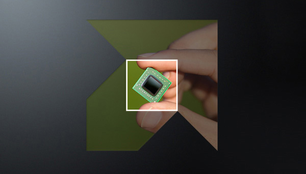
O que é que será que a AMD tem neste novo processo de fabrico, um novo FX ou um novo APU?
-
17-07-15, 16:43 #95O Administrador
- Registo
- Mar 2013
- Local
- Multiverso
- Posts
- 17,814
- Likes (Dados)
- 74
- Likes (Recebidos)
- 156
- Avaliação
- 31 (100%)
- Mentioned
- 31 Post(s)
- Tagged
- 0 Thread(s)
Boas! Post Original de Jorge-Vieira

Espero que seja mesmo um novo FX e a ver se vemos finalmente novas boards com novos chipsets da AMD e socket AM4
Cumprimentos,
LPCMy Specs: .....
CPU: AMD Ryzen 7 5800X3D :-: Board: MSI B550M BAZOOKA :-: RAM: 64 GB DDR4 Kingston Fury Renegade 3600 Mhz CL16 :-: Storage: Kingston NV2 NVMe 2 TB + Kingston NV2 NVMe 1 TB
CPU Cooling Solution: ThermalRight Frost Commander 140 Black + ThermalRight TL-C12B-S 12CM PWM + ThermalRight TL-C14C-S 14CM PWM :-: PSU: Corsair HX 1200 WATTS
Case: NZXT H6 FLOW :-: Internal Cooling: 4x ThermalRight TL-C12B-S 12CM PWM + 4x ThermalRight TL-C14C-S 14CM PWM
GPU: ASUS TUF AMD RADEON RX 7900 XTX - 24 GB :-: Monitor: BenQ EW3270U 4K HDR
-
18-07-15, 15:51 #96Tech Ubër-Dominus
- Registo
- Nov 2013
- Local
- City 17
- Posts
- 30,121
- Likes (Dados)
- 0
- Likes (Recebidos)
- 2
- Avaliação
- 1 (100%)
- Mentioned
- 0 Post(s)
- Tagged
- 0 Thread(s)
AMD Confirms Completing Two 14/16nm FinFET Product Designs – FinFET Based Zen CPUs And Arctic Islands GPUs Due In 2016
AMD’s President and CEO, Lisa Su, revealed at yesterday’s earnings call that AMD has already completed its first couple of FinFET designs. She also stressed that FinFET is going to be incredibly important across all markets for the company in 2016.

Although Su stressed the importance of good design and architecture in making any competitive product as opposed to just manufacturing process. Being on a competitive leading edge process node is undoubtedly important but it’s just a tool. And what the engineers manage to create with that tool in terms of products and innovation is what’s going to matter.
AMD Confirms Completing Two 14/16nm FinFET Product Designs – Will Debut Zen CPUs And Arctic Islands GPUs In 2016
Due to obvious competitive reasons Su did not reveal which products taped out on FinFET. However Su confirmed that AMD’s next generation processors based on Zen as well as the company’s upcoming next generation graphics products – purportedly code named Arctic Islands – are both based on FinFET and are coming out next year. So it’s fair to assume that at least one of the two completed designs is Zen while the other is likely a next generation graphics product set for 2016.
We covered yesterday the slow down of the historic manufacturing process transition cadence as we’ve come to know it in the observation that is Moore’s Law. Intel’s traditional tick-tock cadence has been augmented to take into account this slow down of recent years. 14nm has been challenging for the company and the rest of the industry and 10nm will continue to prove to be challenging. As a result Intel delayed their 10nm Cannonlake family of processors by a year to 2017. And instead will be introducing Kaby Lake as a stop-gap 14nm solution for 2016.
This creates a very interesting dynamic which analysts caught on very quickly. Because it means that for the first time in nearly a decade AMD and Intel will actually have close parity in terms of manufacturing process technology. And will meet for the first time next year with AMD’s launch of its FinFET based Zen CPUs in a similar time-frame to Intel’s Kaby Lake in 2016.
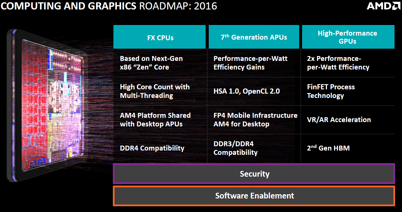
Matt Ramsay – Canaccord Genuity – AnalystAMD seems to be quite confident that Zen is architecturally competitive regardless of the process node. Earlier this year in May we caught a glimpse for the first time into what Zen will bring to the table in 2016. We know Zen will debut on the desktop first on a new socket dubbed AM4 featuring DDR4 memory, a brand new chipset. We also know that Zen processors themselves will feature high core counts, multi-threading and a 40% IPC – instructions per clock – improvement over AMD’s Excavator CPU core. So no doubt it has all the makings of a competitive product.
A little bit of a longer-term strategic question for you, Lisa. Last night, Intel announced the addition of a new chip on their 14-nanometer roadmap and pushed back 10. It strikes me as two things. One, love to get your commentary relative to your foundry partners as to how the [Moore’s Law] progression is going, particularly with Zen coming on 14-nanometer next year. Second, it looks like now you will be in a position to potentially overlap your Zen products with a generation of Intel products that is still on 14-nanometer. Just your reaction to that, in general, and the competitive landscape on the foundry side. Thanks.
Lisa Su – Advanced Micro Devices, Inc. – President & CEO
Matt, I do think the process technology landscape, right now, is quite interesting. On the first part of your question, how do we view FinFET technologies? Actually, I think the maturity of FinFET technologies is coming along very nicely, so we see it as an important part of our roadmap in 2016 across all of our markets. We’ve actually just taped out our first couple of FinFET designs. Relative to what that means for the competitive landscape going forward, I’ve been asked that question a couple of times over the last year and my comments have been, our focus is on design architecture and ensuring that we use all of our design architecture expertise. Zen is a clean sheet design and from architectural standpoint, I think it’s going to be very competitive. The fact that the gap between foundry technologies and other technologies is shrinking, I think does change the competitive landscape and will be a good opportunity as we go forward competitively. We are aggressively going after FinFET and I think that’s going to be an incredibly important node for us.
It looks especially promising considering that Zen will be on a comparable process node to Intel’s Kaby Lake next year and that Zen will bring high core count CPUs to the mainstream. Something that Intel still reserves for the more expensive LGA2011-3 enthusiast platform and will still be limited to Broadwell-E next year. The x86 CPU market has been in a state of chronic stagnation and an aggressive injection of competition may catch Intel by surprise. A good change of pace is needed and AMD seems to be heading in the right direction with Zen.
-
02-08-15, 13:17 #97Tech Ubër-Dominus
- Registo
- Nov 2013
- Local
- City 17
- Posts
- 30,121
- Likes (Dados)
- 0
- Likes (Recebidos)
- 2
- Avaliação
- 1 (100%)
- Mentioned
- 0 Post(s)
- Tagged
- 0 Thread(s)
AMD Reveals the Monsterous ‘Exascale Heterogeneous Processor’ (EHP) with 32 x86 Zen Cores and Greenland HBM2 Graphics on a 2.5D Interposer
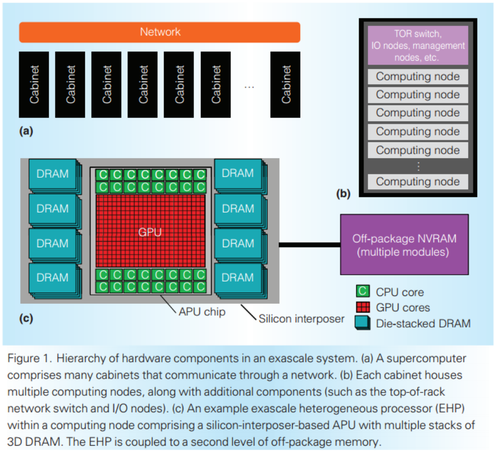
There had been rumors about AMD working on a huge APU with Zen cores and Greenland HBM graphics, something that AMD had hinted upon in its official roadmap. However, it has (finally) officially revealed details about the upcoming APU in a paper submitted to IEEE (Institute of Electrical and Electronics Engineer). The APU, dubbed an “Exascale Heterogeneous Processor” or EHP for short is the mother of all APUs with 32 Zen Cores, an absolutely huge Greenland graphics die and upto 32 GB of HBM2 memory – all on a 2.5D interposer.

Exascale Heterogeneous Processor (EHP) is AMD’s promised monster APU for the HPC segment
The research in question can be found over here and requires paid access, however we were able to get the relevant piece courtesy of Bitsandchips.it. As you may notice, the diagram is a very simple block diagram that doesn’t really reveal much, except the number of CPU cores. Fortunately for us, AMD’s roadmap and the relevant knowledge of HBM technology makes it almost child’s play to identify the exact parts.

Provided the diagram is drawn accurately, the first thing you will note is that there are exactly 32 “CPU Cores”. Since the EHP (APU) is scheduled for 2016-2017, we are most definitely looking at Zen cores (not to mention Excavator cores wouldn’t fit). I can count 4 dies per stack, and since we are dealing with HBM2 at the very least (given the timeframe), these constitute 4-Hi stacks. HBM2 is 8Gb per die, which equates to 4GB per stack (for a 4-Hi stack) in this diagram or a total of 32 GB HBM2 memory onboard the interposer. That’s not it either, memory can be expanded further via the DDR4 channel present on package.
As far as the graphics portion of the Exascale Heterogeneous Processor is concerned, what we know for sure is that this will be the next generation Greenland graphics, what we don’t know is how much the exact core count will will be. Since we have no idea how big Zen Cores actually are (or if the diagram is even drawn to scale) it would be unwise to try to reverse engineer the die size of the GPU from the picture. We can safely say however, that this is one of the hugest GPU dies we have encountered so far. If I were to make a wild guess (caution: speculation) for the sake of giving a number I would say the number of stream processors could easily be above 3072 considering we are talking about a lower process and a huge die.
This brings us to our third deduction. A 2.5D interposer has been used in the EHP (APU) and the CPU and GPU cores all togethery are too numerous (and huge) to have been manufactured as a single die. Not only would the yields on such a monstrosity be beyond imagining, it would be pretty impossible to manufacture such a thing in the first place. The likely conclusion is therefore, that the two compute and graphic portions of the APU are manufactured separately and put together on the interposer later on in assembly (possibly at UMC’s Fab 12 foundry in Singapore, which is already used to assemble Fiji dies). So basically, AMD is fabricating the compute side of the Scale Heterogeneous Processor (EHP) in dies with 16 Zen cores each, for a total of 2 computing and 1 graphics die assembled on the interposer (ignoring the HBM).
Now there has been word on the rumor mill about AMD’s HPC APU for quite a long time and we are fairly certain there will be a 16 core variant as well. Previous leaks have indicated that the processor will be constructed using AMD’s Coherent Fabric – which so happens to be a custom interconnect for the purpose of the cores communicating with the Greenland graphics. Each Zen core will have access to 512KB of L2 cache and 4 Zen cores will share 8MB of L3 cache in the ‘Exascale Heterogeneous Processor’. That equates to a grand total of 16MB L2 Cache and 64 MB L3 cache. Each Zen core will be capable of running two threads (thanks to the company’s shift back to SMT) for a total of 64 threads in this huge APU. The processor is thought to have 8 DDR4 channels with a capacity of 256GB per channel.
Unfortunately for the enthusiasts, there is no guarantee that the EHP will trickle down into consumer variants. Infact, I will be genuinely shocked if it does. Even the 16 core variant that was spotted quite a bit earlier would be hard pressed to enter the mainstream segment. In any case, Heterogeneous Processing is an applause worthy approach to handle the HPC problem. Equipped with Greenland class stream processors for parallel workloads and a small army of Zen cores for the rest, this not-so-tiny APU would be handle just about anything. Not to mention, as the name suggests, the Exascale Heterogeneous Processor is built to be scaled to kingdom come, allowing for a truly powerful rival to Intel’s Xeon Phi coprocessors and even the general GPGPU market.
-
02-08-15, 13:23 #98Master Business & GPU Man
- Registo
- Jan 2015
- Local
- País Campeão Euro 2016
- Posts
- 7,793
- Likes (Dados)
- 0
- Likes (Recebidos)
- 1
- Avaliação
- 41 (100%)
- Mentioned
- 0 Post(s)
- Tagged
- 0 Thread(s)
É bom que se mexam é...
Ideias sem Nexo e Provas do Tráfico de Hardware
"que personifica o destino, equilíbrio e vingança divina." Dejá vú. Que cena!
-
04-08-15, 07:50 #99Tech Ubër-Dominus
- Registo
- Nov 2013
- Local
- City 17
- Posts
- 30,121
- Likes (Dados)
- 0
- Likes (Recebidos)
- 2
- Avaliação
- 1 (100%)
- Mentioned
- 0 Post(s)
- Tagged
- 0 Thread(s)
AMD is researching multi-core ‘exascale heterogeneous processor’
Noticia:Advanced Micro Devices has confirmed that it is researching a multi-core accelerated processing unit based on “Zen” micro-architecture, which will eventually power supercomputers with extreme performance. At present the company is only considering a concept design and it is unclear when AMD decides to actually develop such processor.
AMD, just like many other leading designers of chips, believes that supercomputers with exascale-class performance will have to use hybrid processor that feature both general-purpose cores as well as multiple stream processors found in graphics processing units. AMD has been promoting the idea of hybrid accelerated processing units since 2006, hence, its vision regarding “exascale heterogeneous processor”, which it outlined in a paper published by IEEE, is not surprising.
“To make fully realize the capabilities of the GPU, we envision exascale compute nodes comprised of integrated CPUs and GPUs (i.e., accelerated processing units or APUs) along with the hardware and software support to enable scientists to effectively run their scientific experiments on an exascale system,” the paper reads. “We discuss the hardware and software challenges in building a heterogeneous exascale system, and we describe on-going research efforts at AMD to realize our exascale vision.”
BitsAndChips web-site reports that the concept of EHP [exascale heterogeneous processor] features 16 or even 32 general-purpose cores based on “Zen” architecture, stream processors based on the next iteration of GCN [graphics core next] architecture as well as HBM [high bandwidth memory].
Earlier this year first details about 16-core APU leaked. AMD’s EHP for supercomputers is expected to feature 16 x86 “Zen” cores with two-way simultaneous multi-threading technology and 512KB L2 cache per core, 32MB L3 cache as well as a new-generation “Greenland” graphics engine with ½ double precision compute rate. The exascale heterogenerous processor is also projected to feature a quad-channel DDR4 memory controller with enhanced ECC capabilities that supports up to 256GB of memory per channel, 64 lanes of PCI Express 3.0 that can be used for SATA Express, integrated SATA, 1GbE, USB as well as various legacy interfaces. The APU is also expected to feature on-package 16GB of HBM2 memory with 512GB/s or higher bandwidth. It is assumed that the chip will hit the market in 2017, but AMD has never confirmed this.
AMD confirmed development of a datacenter APU earlier this year, but has never revealed its specifications. Keeping in mind that initial processors based on “Zen” micro-architecture will be made using 14nm FinFET process technology and will not feature more than eight cores, chips with 16 or 32 cores will likely be manufactured using 10nm FinFET fabrication process sometimes in 2018, at the earliest.
http://www.kitguru.net/components/cp...s-gpu-and-hbm/
Mais alguns pormenores sobre estes novos CPUs da AMD baseados na arquiteura ZEN.
-
04-08-15, 11:32 #100O Administrador
- Registo
- Mar 2013
- Local
- Multiverso
- Posts
- 17,814
- Likes (Dados)
- 74
- Likes (Recebidos)
- 156
- Avaliação
- 31 (100%)
- Mentioned
- 31 Post(s)
- Tagged
- 0 Thread(s)
Boas!
No papel parece excelente, já estive a ler o artigo... e parece que finalmente têm uma arquitectura verdadeiramente escalável e flexível.
Agora é preciso é que consigam uma software layer que use os gpus cores como se fossem cpu cores... o que iria ser fantástico, para quem não usar o IGPU para a parte gráfica.
Em alternativa, era usar com o DX12 o HSA e permitir também que a parte do GPU ajudasse em algumas funções a gráfica instalada (seja ela amd ou nvidia).
Cumprimentos,
LPCMy Specs: .....
CPU: AMD Ryzen 7 5800X3D :-: Board: MSI B550M BAZOOKA :-: RAM: 64 GB DDR4 Kingston Fury Renegade 3600 Mhz CL16 :-: Storage: Kingston NV2 NVMe 2 TB + Kingston NV2 NVMe 1 TB
CPU Cooling Solution: ThermalRight Frost Commander 140 Black + ThermalRight TL-C12B-S 12CM PWM + ThermalRight TL-C14C-S 14CM PWM :-: PSU: Corsair HX 1200 WATTS
Case: NZXT H6 FLOW :-: Internal Cooling: 4x ThermalRight TL-C12B-S 12CM PWM + 4x ThermalRight TL-C14C-S 14CM PWM
GPU: ASUS TUF AMD RADEON RX 7900 XTX - 24 GB :-: Monitor: BenQ EW3270U 4K HDR
-
04-08-15, 13:01 #101Tech Ubër-Dominus
- Registo
- Nov 2013
- Local
- City 17
- Posts
- 30,121
- Likes (Dados)
- 0
- Likes (Recebidos)
- 2
- Avaliação
- 1 (100%)
- Mentioned
- 0 Post(s)
- Tagged
- 0 Thread(s)
AMD uses superfast coherent fabric
Noticia:
The next gen Hyper-transport interconnect
AMD has come up with a new interface, interconnect technology it calls coherent fabric.
It is a new inter-chip connection that will be used in the Exascale Heterogeneous Processor (EHP). Coherent fabric is primary interconnect for IP on AMD SOCs, APUs, CPUs and GPUs beginning with the next generation CPU SOC and followed by the Greenland GPU ASIC. Incoherant fabric, on the other hand, is something worn by loud American tourists and is sometimes called a Hawaiian shirt.
AMD's GMI - Global Memory Interconnect, extends the coherent fabric between chips on the same multi-chip module (MCM) package. The coherent fabric extends between packages using combo phys which also support PCIe interconnection.
All this sounds rather complicated, but is basically a faster way for Zen SoC to talk to the Greenland Die on future processors.
Coherent fabric will speed up the communication in Zen CPUs between the cores and cache, host controllers, eg. USB, SATA or GbE, memory controllers, PSP, timer, counter, ACPI or legacy interface, combo phys and GMI layers. GMI phys of Zen die will talk directly with GMI phys of Greenland HBM 2.0 graphics die and uses coherent fabric too.
Our industry sources did not want to go into the specifics of achievable speeds of this interconnect, but the promise of a significant improvement is there. And of course the upcoming AMD's 16 core Heterogenous EHP Processor will benefit from the fast coherent fabric interconnect.
AMD's coherent fabric is the direct competitor to Nvidia's NVlink interconnection that is expected in 2016 with the Pascal GPUs.
http://www.fudzilla.com/news/process...oherent-fabric
Mais uns pormenores interessantes e isto no papel começa a prometer bastante.
-
06-08-15, 10:22 #102Tech Ubër-Dominus
- Registo
- Nov 2013
- Local
- City 17
- Posts
- 30,121
- Likes (Dados)
- 0
- Likes (Recebidos)
- 2
- Avaliação
- 1 (100%)
- Mentioned
- 0 Post(s)
- Tagged
- 0 Thread(s)
AMD's Coherent data fabric enables 100 GB/s
Noticia: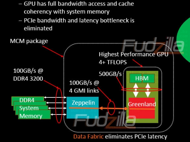
PCIe gives you 15GB/s
After a lot of asking around, we can give you some actual numbers about the AMD's coherent fabric.
The inter-connecting technology already sounded very promising, but now we have the actual number. The HSA, Heterogeneous System Architecture MCM (Multi Chip Module) that AMD is working on can give you almost seven times faster score than the traditional PCIe interface.
Our industry sources have confirmed that with 4 GMI (Global Memory Interconnect) links AMD's CPU and GPU can talk at 100GB/s. the traditional PCIe 16X provides 15GB/s at about 500 ns latency. Data Fabric eliminates PCIe latency too.
AMD will be using this technology with the next gen Multi Chip module that packs a Zeppelin CPU (most likely packed with a bunch of ZEN cores) and a Greenland GPU that of course comes with super fast HBM (High Bandwidth Memory). The Greenland and HBM can communicate at 500 GB/s and can provide highest performance GPU with 4+ teraflops.
This new MCM package based chip will also talk with DDR4 3200 memory at 100GB/s speed making it quite attractive for the HSA computation oriented customers.
http://www.fudzilla.com/news/process...ables-100-gb-s
-
08-08-15, 13:05 #103Tech Ubër-Dominus
- Registo
- Nov 2013
- Local
- City 17
- Posts
- 30,121
- Likes (Dados)
- 0
- Likes (Recebidos)
- 2
- Avaliação
- 1 (100%)
- Mentioned
- 0 Post(s)
- Tagged
- 0 Thread(s)
AMD Publishes Patent for Zen Based APUs with Integrated FPGAs and HBM2 Memory on a 2.5D Interposer
Intel has long since offered a lineup of special processors with FPGAs from Altera onboard. And if a patent that was recently published is to be believed, AMD is planning to do something similar with its future processors as well. With the major addition of having 2.5D stacked HBM2 (memory) at the same time. The target audience of these special CPUs are very specific and usually consist of sometimes semi-custom customers where the load type shifts regularly.

AMD files patent for Zen based processors with FPGAs and HBM2 onboard
FPGAs stand for Field Programmable Gate Arrays. For those not familiar with them, they are a type of processing device that has reconfigurable logic. Basically, you have ASICs which have hard-wired logic, tailored to a specific task and a specific load type allowing them to accomplish said tasks with unparalleled efficiency. Then, you have our modern day CPUs with hard-wired logic that allows many general applications and diverse load types resulting in an all rounder processor capable of doing just about everything – but not very good at certain load types. And finally, you have FPGAs, whose logic is not hard-wired and can be reconfigured accordingly resulting in a very customizable silicon solution for the semi-custom market.
The addition of HBM2 memory would enable AMD offerings to have an edge over Intel’s. While Intel is dabbling in Hybrid Memory Cubes, it has not yet, managed to integrate it into an Xeon FPGA lineup. Also if Zen micro-architecture lives up to its name, it should be more than a match for Intel’s counterparts – especially considering the main requirement for most data-centres and semi-custom servers is energy efficiency (something HBM2 will excel at, not to mention Zen). Infact AMD has already been approached by Facebook to build them a semi custom server processor for their data centres and there is a probability involved (caution: speculation) that this patent might have something to do with that.
HBM2 (memory) offers significant bandwidth upgrades over HBM1 while staying on the same VDD level of 1.2V. And with the advances made (or rather promised) in Zen micro-architecture, the power efficiency of this contraption should be pretty impressive. Unfortunately, like most patents, this one is pretty vague as well, but from what I could gather, the reconfigurable logic (FPGAs) will be an optional intermediary step between the main processor and the memory. Providing the FPGA with custom logic, will allow the user to minimize latency and drastically reduce bottlenecks of any interconnect and get workloads processed almost directly. Its also worth noting that this is almost certainly an APU design – so Greenland graphics should be on the table as well.
-
10-08-15, 13:15 #104Tech Ubër-Dominus
- Registo
- Nov 2013
- Local
- City 17
- Posts
- 30,121
- Likes (Dados)
- 0
- Likes (Recebidos)
- 2
- Avaliação
- 1 (100%)
- Mentioned
- 0 Post(s)
- Tagged
- 0 Thread(s)
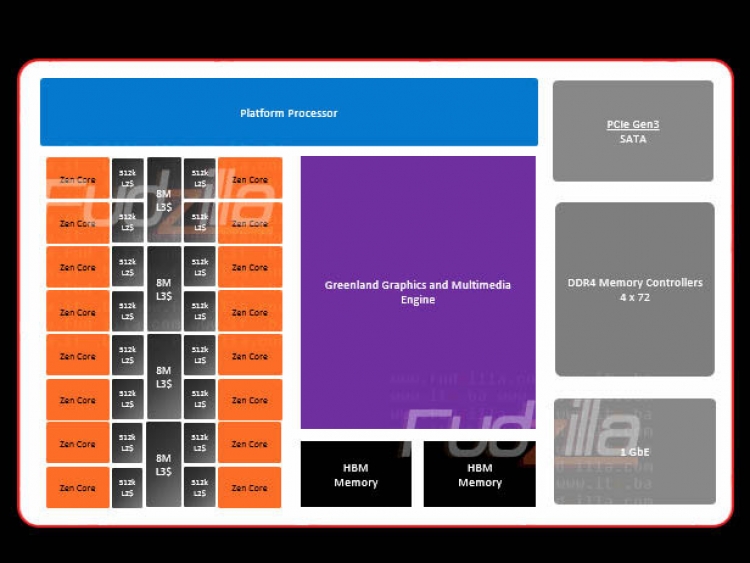
AMD’s Upcoming Opteron MCMs will Pack Zeppelin CPUs and Greenland HBM Graphics with Coherent Data Fabric Support
A recent report by Fudzilla has spilled the beans on the codename of a certain Zen based processor from AMD: “Zeppelin” . If you are reading this, then you probably know the drill (notice the rumor tag above). We have already heard alot about coherent fabric but this leak not only reveals the exact speed of the data fabric but the codename of a processor that will eventually use it as well.
AMD Zeppelin CPUs to use Coherent Data Fabric to communicate with the GPU
I’ll admit I was slightly queasy about this particular rumor – mostly because it reveals too much and too little at the same time. While the source’s history can be considered mostly authentic, this particular slide reveals the codename of a future AMD processor; and since we are talking about an MCM and a custom interconnect, I would be willing to wager this is an Opteron variant. The leak also sheds light on just how much faster Coherent Fabric is from the standard PCIe interface.
The report states that AMD is currently working on a Multi Chip Module that will have a Zeppelin CPU and Greenland GPU connected by Coherent Data Fabric. High Bandwidth Memory (probably on a 2.5D interposer) will be involved as well and will be clocked at 500 GB/s. The homegrown interconnect will support data rates of upto 100GB/s which is alot faster than what the PCIe interface sustains (around 15GB/s). Not only that but latency has been reduced from 500ns to an unknown but allegedly smaller number.

The Zeppelin and Greenland based MCM will feature 4 GMIs or Global Memory Interconnects (which constitute the Coherent Data Fabric I suppose) allowing the CPU to converse with the GPU at 100GB/s. The compute of the GPU is rated at 4.0+ TFlops. Unfortunately, they do not mention whether these are single or double precision numbers and we cant really make any assumptions here either (both are plausible). The MCM itself will contain the GPU and CPU side of things and will talk to the RAM at 100 GB/s as well – allowing for a very HSA friendly environment and minimum bottleneck throughout the whole process.
Previous leaks (from the same source I might add) indicated that the processor will be using AMD’s Coherent Fabric. Each Zen core will have access to 512KB of L2 cache and 4 Zen cores will share 8MB of L3 cache in the ‘Exascale Heterogeneous Processor’. That equates to a grand total of 16MB L2 Cache and 64 MB L3 cache. Each Zen core will be capable of running two threads (thanks to the company’s shift to Simultaneous Multi-Threading). The processor is thought to have 4 DDR4 channels with a capacity of 256GB per channel.
-
13-08-15, 12:52 #105Tech Ubër-Dominus
- Registo
- Nov 2013
- Local
- City 17
- Posts
- 30,121
- Likes (Dados)
- 0
- Likes (Recebidos)
- 2
- Avaliação
- 1 (100%)
- Mentioned
- 0 Post(s)
- Tagged
- 0 Thread(s)
Exclusive details on AMD's Zen
Noticia:
No more shared FPU per two cores
Our well informed industry sources have shared a few more details about the AMD's 2016 Zen cores and not it appears that the architecture won't use the shared FPU like Bulldozer.
The new Zen uses a SMT Hyperthreading just like Intel. They can process two threads at once with a Hyperthreaded core. AMD has told a special few that they are dropping the "core pair" approach that was a foundation of Bulldozer. This means that there will not be a shared FPU anymore.
Zen will use a scheduling model that is similar to Intel's and it will use competitive hardware and simulation to define any needed scheduling or NUMA changes.
Two cores will still share the L3 cache but not the FPU. This because in 14nm there is enough space for the FPU inside of the Zen core and this approach might be faster.
We mentioned this in late April where we released a few details about the 16 core, 32 thread Zen based processor with Greenland based graphics stream processor.
Zen will apparently be ISA compatible with Haswell/Broadwell style of compute and the existing software will be compatible without requiring any programming changes.
Zen also focuses on a various compiler optimisation including GCC with target of SPECint v6 based score at common compiler settings and Microsoft Visual studio with target of parity of supported ISA features with Intel.
Benchmarking and performance compiler LLVM targets SPECint v6 rate score at performance compiler settings.
We cannot predict any instruction per clock (IPC improvement) over Intel Skylake, but it helps that Intel replaced Skylake with another 14nm processor in later part of 2016. If Zen makes to the market in 2016 AMD might have a fighting chance to narrow the performance gap between Intel greatest offerings.
http://www.fudzilla.com/news/process...bout-amd-s-zen
Mais pormenores interessantes que deixam antever que esta nova arquitetura da AMD promete bastante, outro pormenor que também começa a ficar evidente é uma clara aproximação aos processos da Intel utilizados nos core i5/i7.

 Responder com Citação


Informação da Thread
Users Browsing this Thread
Estão neste momento 1 users a ver esta thread. (0 membros e 1 visitantes)
 Regras
São agora 05:13.
 User Alert System provided by
Advanced User Tagging v3.3.0 (Lite) -
vBulletin Mods & Addons Copyright © 2024 DragonByte Technologies Ltd.
User Alert System provided by
Advanced User Tagging v3.3.0 (Lite) -
vBulletin Mods & Addons Copyright © 2024 DragonByte Technologies Ltd.
Feedback Buttons provided by Advanced Post Thanks / Like (Lite) - vBulletin Mods & Addons Copyright © 2024 DragonByte Technologies Ltd.
Portugal-Tech 2012-24 | Todos os direitos reservados! Alojamento Powered by: Trignosfera
Powered by vBulletin® Version 4.2.5 Alpha 3
Copyright © 2024 vBulletin Solutions, Inc. All rights reserved.
Copyright © 2024 vBulletin Solutions, Inc. All rights reserved.
Feedback Buttons provided by Advanced Post Thanks / Like (Lite) - vBulletin Mods & Addons Copyright © 2024 DragonByte Technologies Ltd.
Portugal-Tech 2012-24 | Todos os direitos reservados! Alojamento Powered by: Trignosfera
Bookmarks