

SK Hynix confirms mass production of first-gen HBM memory
Noticia:SK Hynix, one of the worlds major producers of memory, on Tuesday said that it had begun volume shipments of its high-bandwidth memory (HBM) designed for bandwidth-demanding applications. The first products to use HBM will be AMDs Radeon R9 Fury-series graphics cards, but eventually other devices will utilize the new memory type as well.
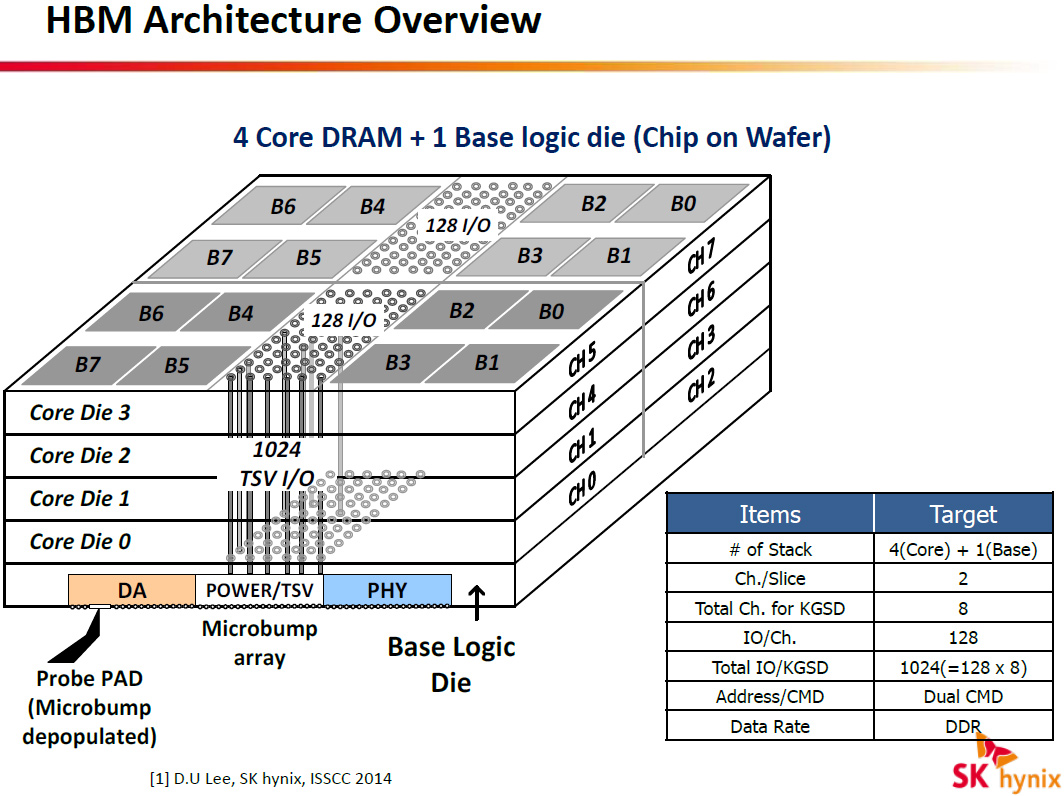
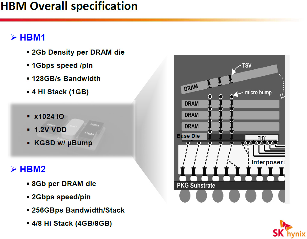
The first-generation HBM (HBM1) memory (which complies with JEDECs JESD235 standard) stacks four DRAM dies with two 128-bit channels per die on a base logic die, which results into a memory device with a 1024-bit interface. Each channel is similar to a standard DDR interface, but is completely independent and therefore each channel within one stack and even within one die can operate at different frequency, feature different timings and so on. HBM devices require 1.2V voltage.
The first-gen HBM uses 2Gb DRAM dies and thus can form only 1GB 4Hi stack (4 high stack) packages. Each HBM 4Hi stack provides 128GB/s of bandwidth. HBM memory chips are tested before shipping to customers by SK Hynix. Each HBM 4Hi stack is placed on an interposer next to the graphics processing unit, for the first time in the industry. The first-gen HBM stacks are made using a proven 29nm fabrication process.
AMD has pioneered the adoption of HBM1 technology in graphics applications achieving unprecedented memory bandwidth while reducing memory subsystem power said Joe Macri, corporate vice president and product CTO at AMD, Integrating AMDs graphics processing unit and HBM1 on a single 2.5D silicon interposer represents a major step forward in high performance graphics applications.
Even though the first-generation HBM has a number of limitations when it comes to the amount of stacks (only four layers are supported) and capacities of DRAM channels, AMD believes that unprecedented bandwidth provided by such chips 512GB/s will help it to significantly improve performance of its Radeon Fury X graphics solutions compared to current-gen solutions.
SK Hynix is shipping HBM to AMD today and plans to support demand for such memory from other customers.
Next year SK Hynix and other memory producers will start to manufacture second-generation HBM that will support up to eight memory stacks, higher DRAM capacities and clock-rates. HBM2 will allow to create 8GB memory chips with 256GB/s bandwidth per chip.
High bandwidth memory technology is the first JEDEC standard memory targeted for interposer system-in-package applications, effectively breaking down the memory wall barrier through tight integration of DRAM and high performance processors said Kevin Widmer, vice president of technical marketing at SK Hynix America. The performance requirements of emerging graphics, computing and networking applications are driving the demand for High bandwidth memory.
http://www.kitguru.net/components/gr...en-hbm-memory/
Fica aqui o topico para se debater sobre este tema das novas memórias que vão estar presentes nas placas graficas das proximas gerações.

User Tag List
 Likes: 0
Resultados 1 a 15 de 20
Tópico: HBM - High bandwich Memory
-
17-06-15, 08:32 #1Tech Ubër-Dominus


- Registo
- Nov 2013
- Local
- City 17
- Posts
- 30,121
- Likes (Dados)
- 0
- Likes (Recebidos)
- 2
- Avaliação
- 1 (100%)
- Mentioned
- 0 Post(s)
- Tagged
- 0 Thread(s)
HBM - High bandwich Memory
-
17-06-15, 10:04 #2Tech Veterano

- Registo
- May 2014
- Local
- LPPT
- Posts
- 5,187
- Likes (Dados)
- 0
- Likes (Recebidos)
- 3
- Avaliação
- 7 (100%)
- Mentioned
- 0 Post(s)
- Tagged
- 0 Thread(s)
HBM: entenda como funcionam as novas memórias 3D da AMD
Chega de rumores e especulações. Hoje, a AMD finalmente revelou as informações oficiais sobre as memórias gráficas que equiparão sua futura linha de placas de vídeo.
A sigla HBM, que dá nome ao novo tipo de chip de memória, faz referência justamente à principal vantagem dela: a alta largura de banda de memória.
Na verdade, alguns detalhes sobre o funcionamento desses componentes circulam na web faz algum tempo, até porque a própria AMD já havia mostrado detalhes dos novos chips de memória. A diferença é que agora temos informações concretas e podemos compreender como a HBM funciona e de que forma ela vai melhorar o desempenho gráfico dos PCs.
A evolução se faz necessária
Primeiramente, devemos compreender como funciona as atuais placas de vídeo. Ao observar uma placa sem o dissipador, você pode rapidamente identificar que a GPU (o chip gráfico) está localizado no centro de tudo.
Talvez, nas placas mais modernas, não seja possível identificar visualmente as trilhas eletrônicas, já que elas ficam no meio da placa, mas em modelos antigos é possível visualizá-las rapidamente. A unidade de processamento gráfico está conectada a quase todos os componentes que ficam ao seu redor.
Essas trilhas são como linhas bem fininhas desenhadas na placa, por onde os dados irão trafegar de um lado para outro. As informações que ficam armazenadas na memória gráfica são solicitadas pela GPU, que processa os dados de acordo com as actividades realizadas pelo jogador. Da mesma forma que alguns dados são enviados para o chip de vídeo, outros saem dali e vão para a memória é uma comunicação rápida e constante.
Até agora, com a tecnologia GDDR5, os processadores gráficos realizam a comunicação através de uma grande quantidade de vias paralelas, estabelecendo a comunicação através de interfaces de até 512 bits como vemos em placas como a Radeon R9 295X2.
É importante ressaltar que cada chip usa interface de 32 bits (entrada e saída de dados), mas o total de chips resulta na interface total. Geralmente, para calcular a interface sem precisar perder tempo, basta contar os chips de memória da placa de vídeo e multiplicar por 32. No caso da Titan X, temos 12 chips, o que significa que no total ela tem uma interface de 384 bits.
Mesmo distribuindo as trilhas para várias direções, a quantidade delas acaba sendo limitada pelo espaço físico. Além disso, apesar de a adoção de esquemas inteligentes de disposição dos chips de memória solucionar esse inconveniente parcialmente, o posicionamento dos componentes e a limitação de espaço se tornam fatores de complicação.
Como resolver? Layouts maiores já vêm sendo adoptados, mas as placas de vídeo começaram a ocupar espaço exagerado dentro dos gabinetes. Com o advento da expansão da quantidade de memória de vídeo, as fabricantes optaram por chips de maior capacidade, mas isso logo também se mostrará um problema.
Mas ora TecMundo, não dá para evoluir as memórias sem mexer na interface da memória? Sim, dá para melhorar a performance da memória sem ampliar o número de vias, sendo necessário apenas aumentar a frequência desses componentes. Acontece que aí caímos em outro problema: o aumento de temperatura e de consumo de energia.
Uma arquitectura completamente diferente
Visando evitar transtornos e antecipar a limitação da actual tecnologia, a AMD tem trabalhado há alguns anos, em parceria com a Hynix e a JEDEC, no desenvolvimento de uma nova memória. A HBM parte para um princípio completamente diferente, que já é possível notar na parte física da placa de vídeo.
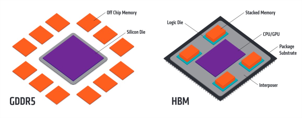
Em vez de chips dispostos lado a lado na placa de circuito impresso (PCB), os módulos de memória nesse novo tipo de arquitectura são empilhados, como se fosse um prédio de memória.
A comunicação agora acontece em duas direcções: dentro da pilha de memória através de vias internas e com o chip gráfico usando as vias da placa de vídeo. Na imagem acima, você pode compreender o esquema de layout do HBM e verificar a existência das vias internas de comunicação.
De acordo com os slides oficias da AMD, a memória HBM não é apenas um chip em cima do outro. O esquema é bem mais inteligente, com direito a um componente (interposer) que conecta substrato, GPU, processador lógico e módulos.
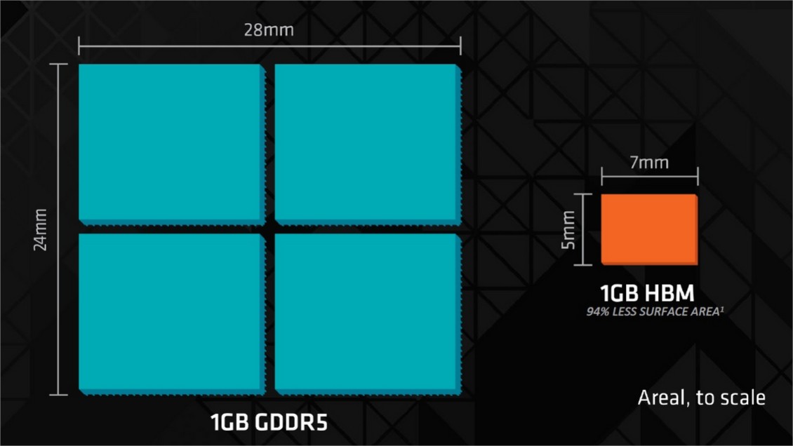
Com a adopção deste layout empilhado, a AMD poderá economizar um espaço significativo na placa de vídeo. A memória HBM é muito mais compacta, utilizando até 94% menos espaço da superfície do PCB.
Cada pilha HBM de 1 GB mede apenas 5 mm de comprimento e 7 mm de largura. A mesma quantidade de memória com tecnologia GDDR 5 ocupava até 24 mm de comprimento e 28 mm de largura. Essa redução no tamanho das pilhas de memória HBM deve ajudar na criação de placas de vídeo mais compactas.
Essa nova forma de comunicação permite aumentar a interface da memória, saindo do padrão de 32 bits e passando para 1.024 bits por pilha de memória. Como você pode imaginar, com essa alteração, automaticamente temos uma mudança na largura de banda da memória. Segundo a Hynix, cada pilha pode transferir até 128 GB/s. É muita coisa!
É curioso notar, contudo, que a AMD prefere manter os números baixos. A informação oficial da fabricante dos chips Radeon informa que a largura de banda será superior aos 100 GB/s.
Pois é, por ora, a AMD informa que os chips HBM trabalharão na frequência dos 500 MHz (chegando a 1 Gbps) enquanto que a memória GDDR5 trabalha a 1.750 MHz (e chega a 7 Gbps). Aí você pensa: nossa, TecMundo, então a memória GDDR5 é melhor?. Veja bem, nem tudo é clock no mundo do hardware. Nesse caso, a frequência é compensada pela interface.
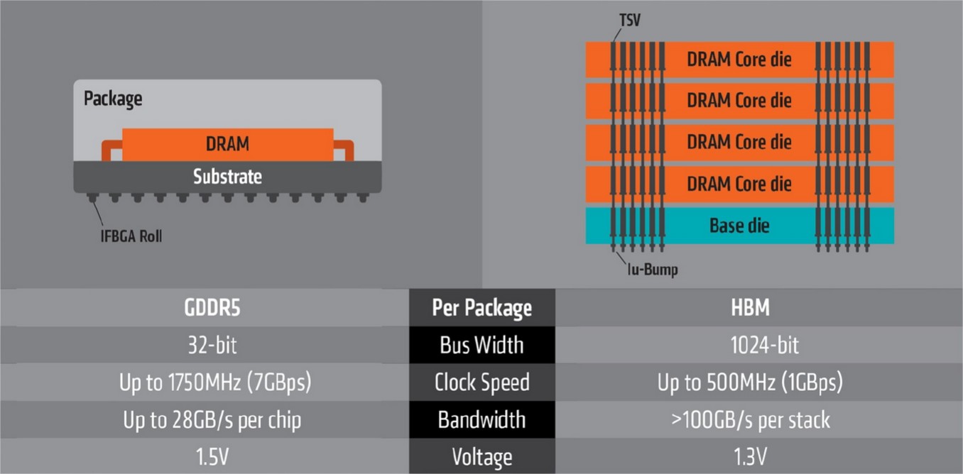
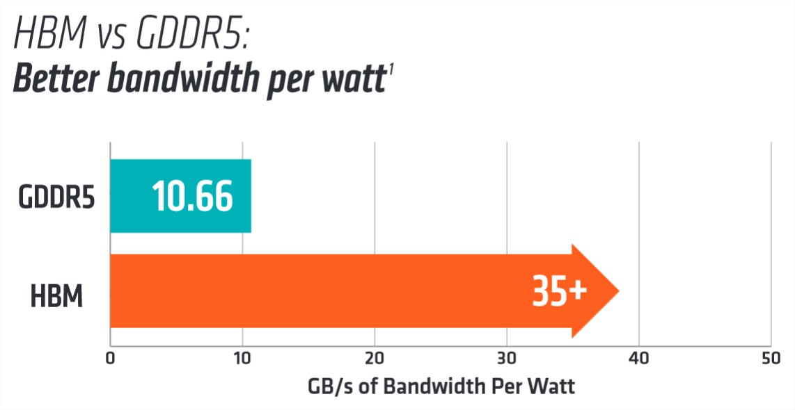
Para finalizar, além de todas essas melhorias, temos a questão da tensão de operação. As memórias GDDR5 trabalhavam com 1,5 volts, as memórias HBM, por outro lado, funcionarão com apenas 1,3 volts. Isso significa que elas serão muito melhores do ponto de vista energético e devem apresentar temperaturas favoráveis para trabalho intenso.
E a capacidade de armazenamento?
É importante ressaltar que a apresentação oficial da HBM não é exactamente uma introdução à nova série de chips Radeon. Todavia, a AMD acabou revelando uma informação que diz respeito a sua nova placa de vídeo top de linha (que deve ser a R9 390X): a capacidade de armazenamento dos chips.
Tal qual um disco rígido, a memória RAM também serve para guardar arquivos. Sua função essencial é armazenar informações, mas apenas de forma temporária. O número que você vê destacado nas embalagens e que muitos vendedores ressaltam como se fosse um indicador de desempenho é na verdade apenas a capacidade para guardar dados temporariamente.
De qualquer forma, ter conhecimento desse número é de suma importância, já que ele dita o quanto de informações pode ser armazenado para que a GPU processe e você tenha resultados mais agradáveis. Por exemplo: você provavelmente não conseguirá rodar um jogo em resolução 4K com uma placa que tem apenas 2 GB de memória.
Para entender é bem simples: as texturas dessa resolução ocupam um espaço virtual astronómico, sendo que a placa de vídeo não tem onde guardar esses dados. Sendo assim, gostamos de ter acesso antecipado a esse tipo de informação quanto aos chips HBM da próxima linha de produtos da AMD.
Conforme a fabricante revelou, cada pilha de memória HBM tem 4 chips de 256 MB, o que totaliza 1 GB por pilha. Inicialmente, a AMD pretende instalar 4 pilhas dessa em suas novas placas, o que significa que teremos um total de 4 GB nas próximas Radeons.
Pode parecer um número estrondoso, mas, apenas para fins especulativos, na prática pode ser que essa quantidade não seja suficiente para trabalhar com os tantos filtros e recursos gráficos na resolução 4K em jogos mais recentes não é por acaso que a TITAN X tem 12 GB.
É claro que enquanto não tivermos o produto em mãos não podemos dar certeza de nada, portanto pode ser que acabemos queimando nossa língua. E também devemos ressaltar que essa limitação de capacidade pode ser amenizada pela largura de banda expandida e também pela nova API da Microsoft que deve optimizar o uso da memória gráfica.
Por fim, temos que ressaltar que essa questão da quantidade de memória deve ser algo temporário, adoptado apenas na primeira geração da tecnologia HBM. Na próxima versão, é bem possível que a AMD já parta para uma solução com o dobro de memória de vídeo.
A AMD deve anunciar sua nova série de placas de vídeo na Computex, que começa já no dia 2 de Junho. A fabricante promete dar muitos detalhes sobre os novos produtos, sendo que essa apresentação da HBM servirá apenas como base de apoio para que o público compreenda os benefícios da nova geração de chips Radeon. O que será que vem por aí?
Fonte: Tecmundo
Leitura interessante.i7-4790K + NZXT Kraken X52 | Z97 MSI GAMING 7 | EVGA FTW3 ICX 1080 Ti | GSkill RIPJAW Z 16 GB DDR3 2133MHZ CL9 | SSD Crucial MX100 250GB + SEAGATE 3TB + M.2 KINGSTON M2 120GB | SOUND BLASTER Z | EVGA G2 SUPERNOVA 1000W | SAMSUNG 32´ UH850
-
19-06-15, 15:17 #3Tech Ubër-Dominus
- Registo
- Nov 2013
- Local
- City 17
- Posts
- 30,121
- Likes (Dados)
- 0
- Likes (Recebidos)
- 2
- Avaliação
- 1 (100%)
- Mentioned
- 0 Post(s)
- Tagged
- 0 Thread(s)
Is HBM Memory Production Affecting Availability of AMD Fury Series GPUs?
Noticia: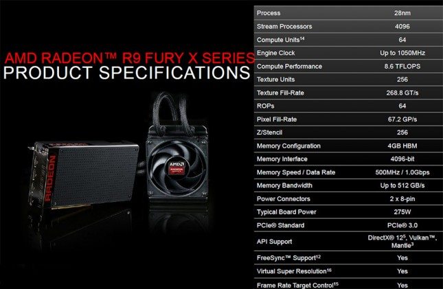
Being in the industry, it’s not uncommon for us to hear little snippets of information, rumours and a heck of a lot of top-secret stuff, but sometimes, that information comes together and gives us a unique insight into what goes on behind the scenes. As many of you will know, the incredible AMD Radeon Fury and the Fury X graphics cards are soon to be released. What you likely don’t know, is that many sites, including eTeknix, likely won’t have a review on launch day. It’s fairly standard practice for sites like us to have the hardware pre-release, with few exceptions, but it seems the Fury series is being handled very differently by AMD.
We’ve caught word that the Fury cards won’t be going out for review, but also that the Fury X will only get 10 samples for the whole of the EU, reviewers will keep the cards for no more than two days, then cycle them around to the next set of reviewers. This fits in with earlier rumours we’ve heard that HBM is exceedingly difficult to produce, as well as rumours that retail stock will be in very short supply due to these manufacturing difficulties. Could it be that AMD simply don’t have enough cards to go around? From what we understand, that certainly seems to be the case. Industry sources are already whispering to us that those actually wanting to buy the card will need luck on their side. This issue will no doubt be impacted even further by the expected high demand for the new card.
So for now, we won’t be able to bring you benchmarks of the new card, but we’re certainly working hard to find a way to do so. Hopefully, we can get the right information to you, our readers, should you be eager to see how well this card performs in a real world environment before purchase; if you can find stock that is.
We’ll keep you updated as soon as we have more information.
http://www.eteknix.com/hbm-memory-pr...y-series-gpus/
-
20-08-15, 16:04 #4Tech Ubër-Dominus
- Registo
- Nov 2013
- Local
- City 17
- Posts
- 30,121
- Likes (Dados)
- 0
- Likes (Recebidos)
- 2
- Avaliação
- 1 (100%)
- Mentioned
- 0 Post(s)
- Tagged
- 0 Thread(s)
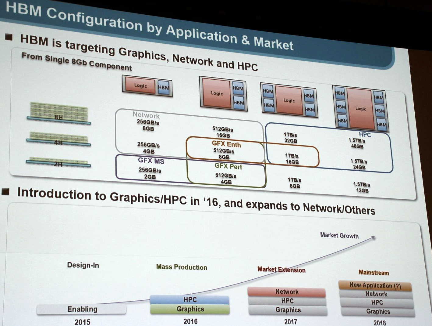
Samsung Enters The HBM Market In 1H 2016 – HPC and GPU Ready HBM With Up to 1.5 TB/s Bandwidth and 48 GB VRAM
At IDF15, Samsung announced that they will commence mass production of HBM stacked memory starting early 2016. High Bandwidth Memory or HBM in short, is the name of the latest memory chips that will be integrated in a wide array of products and devices. Co-developed by TSMC and AMD, the HBM chips were first fused on the Radeon R9 Fury X graphics card from AMD that launched in June 2015.


Image Credits: ComputerbaseSamsung To Commence Mass Production of HBM Memory in Early 2016
The Radeon R9 Fury X debuted with 4 GB of HBM memory which was arranged in layers of four die stacks, each of which was 4-stacks high and each die had 1 GB of VRAM. Each HBM stack had a 1024-bit wide bus while the whole thing had a large 4096-bit wide bus that was clocked at 500 MHz (1.0 GHz effective) clock to deliver 512 GB/s memory bandwidth. The bandwidth improvement for HBM is quite huge even though the difference in performance between GDDR5 and HBM (at the moment) is quite low since high-end graphics cards have large pools of bandwidth already available to them that isn’t being utilized to full extent. We saw some benchmarks of the Radeon R9 Fury X with its HBM overclocked to pump out 1 TB/s bandwidth but the overclocker reported not much benefit from the HBM overclock, the graphics chip on the other hand when overclocked featured a greater impact on performance. HPC applications that use HBM will show the actual advantage when several Terabytes of bandwidth gets effectively utilized to power intense workloads and graphics demand.
With Samsung entering the HBM field, we can see a large influx of new HBM powered processors and devices. Samsung is going all out to bring several tiers of HBM stacked memory to the graphics can HPC market. Starting in 2016, the first markets that Samsung will focus towards will include the HPC and graphics department. Samsung has a wide array of HBM configurations pre-planned. Each HBM stack will be made from a single 8Gb component and range down to several tiers of HBM SKUs. The entry level models include the 2-Hi DRAM model that will be integrated on mainstream 2 GB HBM graphics cards (256 GB/s), performance based graphics with 4 GB HBM (512 GB/s). The Enthusiast graphics cards will ship with 4-Hi DRAM with 2 HBM stacks that will allow 8 GB VRAM (512 GB/s) and finally, 4 HBM Stacks with 16 GB VRAM models (1 TB/s).
On the HPC front, there are a wide array of high bandwidth and dense memory designs that include 4-Hi DRAMs with 4 HBM stacks that feature 32 GB VRAM (1 TB/s) and the bulky, 8-Hi DRAMs configured in 6 HBM stacks with 24 GB and 48 GB VRAM, both models featuring 1.5 TB/s bandwidth. There are also some network oriented HBM SKUs which are planned for launch in 2017 with 8-Hi DRAM Stacks configured in 1-2 HBM chips. In 2018, Samsung wants to focus on increase market growth by entering new applications to incorporate their HBM designs.

For all good, HBM seems to be the way forward and the mainstream applications of HBM memory sound great for mainstream and performance oriented graphics cards that are going to arrive in 2016. We know that NVIDIA has a full fledged FinFET based Pascal lineup coming out in 2016 which is rumored to feature 32 GB of HBM and 17 Billion transistors while AMD has their Arctic Islands planned for launch the same year that will finally bring a completely new GCN architecture based graphics lineup. It was previously rumored that TSMC might give AMD priority on access to HBM for their next graphics lineup so Samsung entering the HBM market will bode quite well for NVIDIA. Overall, this sounds great and we can’t wait to see Samsung kick start their production of HBM memory.
-
22-08-15, 14:16 #5Tech Ubër-Dominus
- Registo
- Nov 2013
- Local
- City 17
- Posts
- 30,121
- Likes (Dados)
- 0
- Likes (Recebidos)
- 2
- Avaliação
- 1 (100%)
- Mentioned
- 0 Post(s)
- Tagged
- 0 Thread(s)
Samsung expects graphics cards with 6144-bit bus, 48GB of HBM memory onboard
Noticia:Samsung Electronics indicated that it plans to start volume production of high-bandwidth memory (HBM) next year at the Intel Developer Forum this week. At the trade-show, the company revealed its current vision and expectations concerning HBM. Samsung foresees that eventually high-performance applications (such as GPUs) could feature up to six HBM devices to enable unprecedented capacities and bandwidth.
As it appears, Samsung plans to skip the first-generation HBM memory and will only manufacture products compliant with the second-generation HBM specification, which offers higher densities and clock-rates. Such approach will let Samsung to address broader market segments with its HBM offerings. Right now HBM can only be used on consumer graphics cards and certain highly-custom products, but HBM2 will enable professional and high-performance computing GPU-based solutions, which require a lot of memory onboard.
Samsung is currently working on multiple HBM packages featuring two (2Hi stack), four (4Hi) and eight (8Hi) 8Gb memory devices on a base logic die with 1024-bit interface, according to a slide that the company demonstrated at the IDF (which was published by ComputerBase.de). Maximum data-rates of Samsung’s HBM products will be 2Gb/s, which will support up to 256GB/s of bandwidth per chip.
Samsung believes that HBM memory will enable it to create a variety of chip offerings targeting different market segments. Designers of logic chips (GPUs, APUs, network processors, etc.) will be able to integrate the right amount of HBM controllers into their chips in order to target different applications. At present AMD’s “Fiji” graphics processing unit supports up to four HBM stacks over its 4096-bit interface. Eventually, logic chips could accommodate more HBM controllers and expand interface width to unprecedented 6144-bit, according to Samsung Electronics.
For example, a mainstream graphics card could use just one 2Hi HBM chip to accommodate a 2GB frame-buffer with 256GB/s bandwidth. More advanced graphics adapters for consumers and creative professionals could feature four 2Hi or four 4Hi HBM stacks that provide up to 1TB/s of bandwidth as well as 8GB, 16GB or 32GB of memory. Accelerators for high-performance computing as well as ultra-high-end GPU offerings will support six HBM stacks, thus enabling cards with 12GB, 24GB or 48GB of onboard memory with 1.5TB/s bandwidth.
So far, neither AMD nor Nvidia have demonstrated even hypothetical product implementations (which are used to showcase potential future uses of technologies) of GPU-based solutions featuring six HBM memory chips. Intel Corp.’s Xeon Phi co-processors use HMC [hybrid memory cube] DRAMs as “near memory” and are not expected to support HBM any time soon.
Samsung expects HBM memory to be used for consumer graphics cards and high-performance computing accelerators based on AMD “Arctic Islands” and Nvidia “Pascal” graphics processors next year. Sometimes in 2017, network products will also take advantage of the new memory type. Three years from now other applications could employ HBM, according to Samsung.
The world’s largest maker of dynamic random access memory (DRAM) did not unveil any details about its actual HBM chips (capacities, clock-rates, etc.), but expect a family of products with different densities and frequencies.
Samsung did not disclose which process technology it will use to manufacture HBM.
http://www.kitguru.net/components/gr...emory-onboard/
Muito provavelmente aquele enormidade de BUS seja uma realidade nos proximos meses com as proximas gerações de graficas da nVidia e AMD.
-
26-08-15, 15:59 #6Tech Ubër-Dominus
- Registo
- Nov 2013
- Local
- City 17
- Posts
- 30,121
- Likes (Dados)
- 0
- Likes (Recebidos)
- 2
- Avaliação
- 1 (100%)
- Mentioned
- 0 Post(s)
- Tagged
- 0 Thread(s)
Samsung making HBM 2 memory in 2016
Noticia: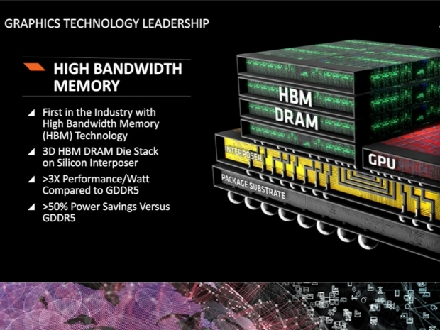
The future of graphics
High Bandwidth Memory (HBM) will define the future of graphics and it looks like Samsung will be ready to release products using the technology soon.
Our friends at Computerbase have broken the story about Samsung making High Bandwidth Memory HBM 2 memory. HBM 2.0 will find its way to HPC and Graphics cards in 2016 and Samsung expects that by 2017 this super-fast type of memory will reach the network market. The plan is to see HBM 2.0 mainstream by 2018.
Our well placed, camera shy sources within the computer graphics industry have confirmed that SK Hynix and Samsung will be providing the memory for graphics cards in 2016. Hynix has started shipping the first generation HBM to AMD for its Fury X products and has a head start over Samsung.
Usually Samsung doesn’t fall that far behind and is quick to learn. We hear that both companies are competing for graphics cards designs in the 2016.
AMD has the Greenland high end GPU lined up while Nvidia has pinned its hopes in its first ever High Bandwidth Memory 2.0 product codenamed Pascal.
The second generation HBM offers 8Gb per DRAM die, 2Gbps speed per pin, 256 GB/s bandwidth and Four Hi Stack of 4GB or 8 Hi Stacks of 8GB per chip.
HBM2 means that there can be cards with four HBM 2.0 chips, 4GB per chip, or four HBM 2.0 chips with 8GB per chip. This results in 16GB and 32GB cards. This sounds like an appropriate amount of memory for high end GPU in 2016.
It was naive to believe reports that AMD will have SK Hynix love since it had a head start with the Fiji codenamed Fury X branded cards. Nvidia has close to 80 percent of the market, memory manufacturers including SK Hynix or Samsung cannot ignore that. They are in the business of making money.
http://www.fudzilla.com/news/graphic...memory-in-2016
-
29-08-15, 14:02 #7Tech Ubër-Dominus
- Registo
- Nov 2013
- Local
- City 17
- Posts
- 30,121
- Likes (Dados)
- 0
- Likes (Recebidos)
- 2
- Avaliação
- 1 (100%)
- Mentioned
- 0 Post(s)
- Tagged
- 0 Thread(s)
AMD started to work on HBM technology nearly a decade ago
Noticia:The high-bandwidth memory (HBM) introduced along with AMD’s code-named “Fiji” graphics processing unit radically changes the way graphics adapters are built and also dramatically improves potential performance of future graphics processing units. But while HBM looks ingeniously simple on paper, it was extremely hard to develop and is not easy to build. In fact, AMD started to work on what is now known as HBM as early as in 2006 – 2007.
The need for speed
Memory bandwidth has been a performance-limiting factor for graphics processors since the introduction of the first gaming-grade graphics cards, three-dimensional games and 32-bit colour back in the nineties. In a bid to considerably increase performance of a graphics adapters, IHVs [independent hardware vendors] had to bolster bandwidth of their DRAM [dynamic random access memory], which was not always easy.
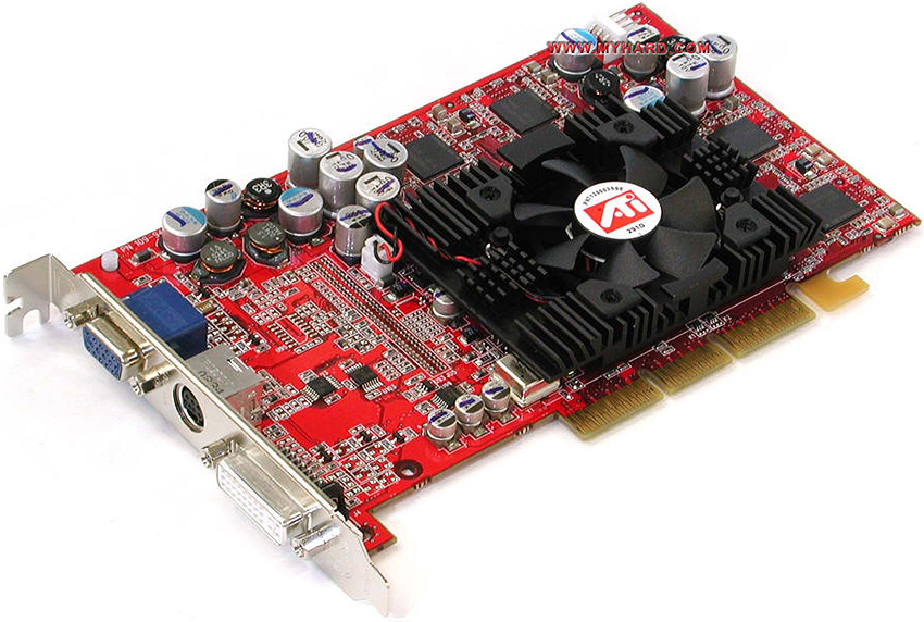 ATI Radeon 9700 Pro: World’s first graphics card with 256-bit memory bus. Image by myhard.com.
There are several ways to increase memory bandwidth on a graphics card: to rise memory clock-rate, to widen memory interface, or to use a more efficient memory technology. After increasing frequencies of graphics DRAM to rather high levels in 1997 – 1998, Nvidia Corp. was the first company to start using the double data rate (DDR) memory (which transfers data on both the rising and falling edges of the clock signal, the technology known as double-pumping) on its GeForce 256 DDR graphics cards in 1999 and doubled bandwidth available to the GPU. ATI Technologies introduced the world’s first graphics card with 256-bit memory bus in 2002 and doubled memory bandwidth of graphics processors once again. In 2002 – 2003 new memory technologies – GDDR2 and GDDR3 – designed specifically for GPUs and supporting quad-pumping were introduced and doubled available bandwidth another time.
But memory bandwidth improvements in the early 2000s did not come for free. Increases of clock-rates and data rates amplified power consumption of memory chips. Wider memory interfaces required more memory ICs, which also increased power requirements of add-in-boards.
By 2006 – 2007, when the work on the ATI R600 graphics processor with 512-bit memory bus as well as on the GDDR4 and the GDDR5 memory technologies was essentially completed, it became clear that memory consumed a lot of power already and would consume even more over time. Since ATI and Nvidia planned to use their GPUs for high-performance computing (HPC) applications, which require a lot of local memory, it was obvious that power consumption of GDDR was going to become a problem.
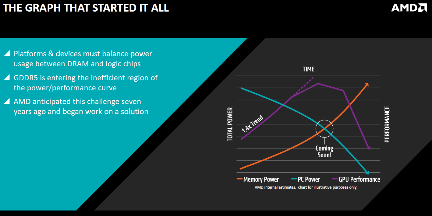
At the time, new memory tech development team at ATI Technologies led by Joe Macri came up with an idea of brand-new memory technology, which could provide extreme bandwidth while consuming a low amount of energy. The key elements of the new technology were multi-layer memory devices with an ultra-wide interfaces that used silicon interposer to connect to a processing device.
Brief history of HBM
Modern technologies take a long time to develop. For example, the work on DDR4 started back in 2005, a couple of years before DDR3 was commercially launched. Similarly, ATI Technologies (which AMD acquired in 2006) started to think about high-bandwidth memory with low power consumption about a decade ago, before the company helped to commercialize GDDR4 in 2006 and GDDR5 in 2008. The work on what is now known as HBM began sometimes in 2006 – 2007 and in 2013 the technology became an industry standard.
Architecturally, the first-generation high-bandwidth memory (JESD235) uses a protocol similar to that of the original DDR, which development kicked off in 1996 and was concluded in mid-2000. But a in a bid to finish the new standard, AMD, SK Hynix and other developers had to create a massive amount of additional technologies that ultimately facilitated creation of graphics processors like AMD’s “Fiji”.
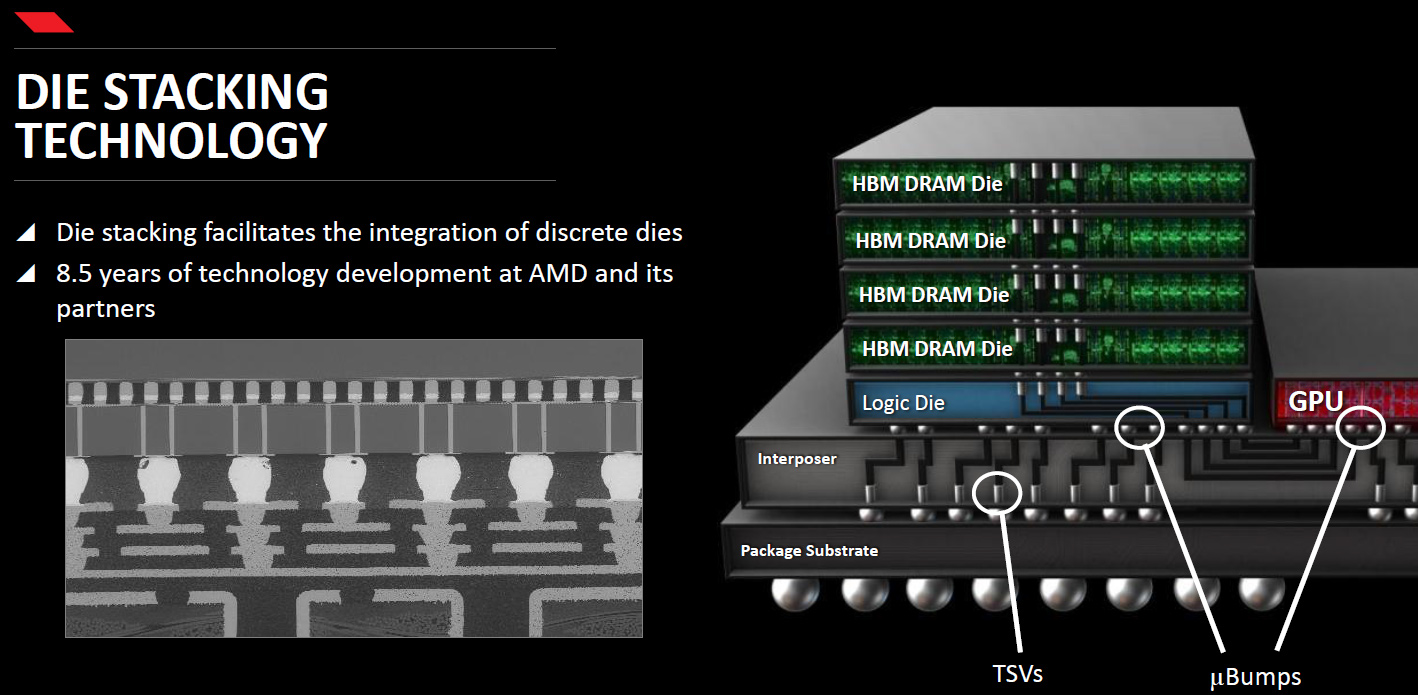
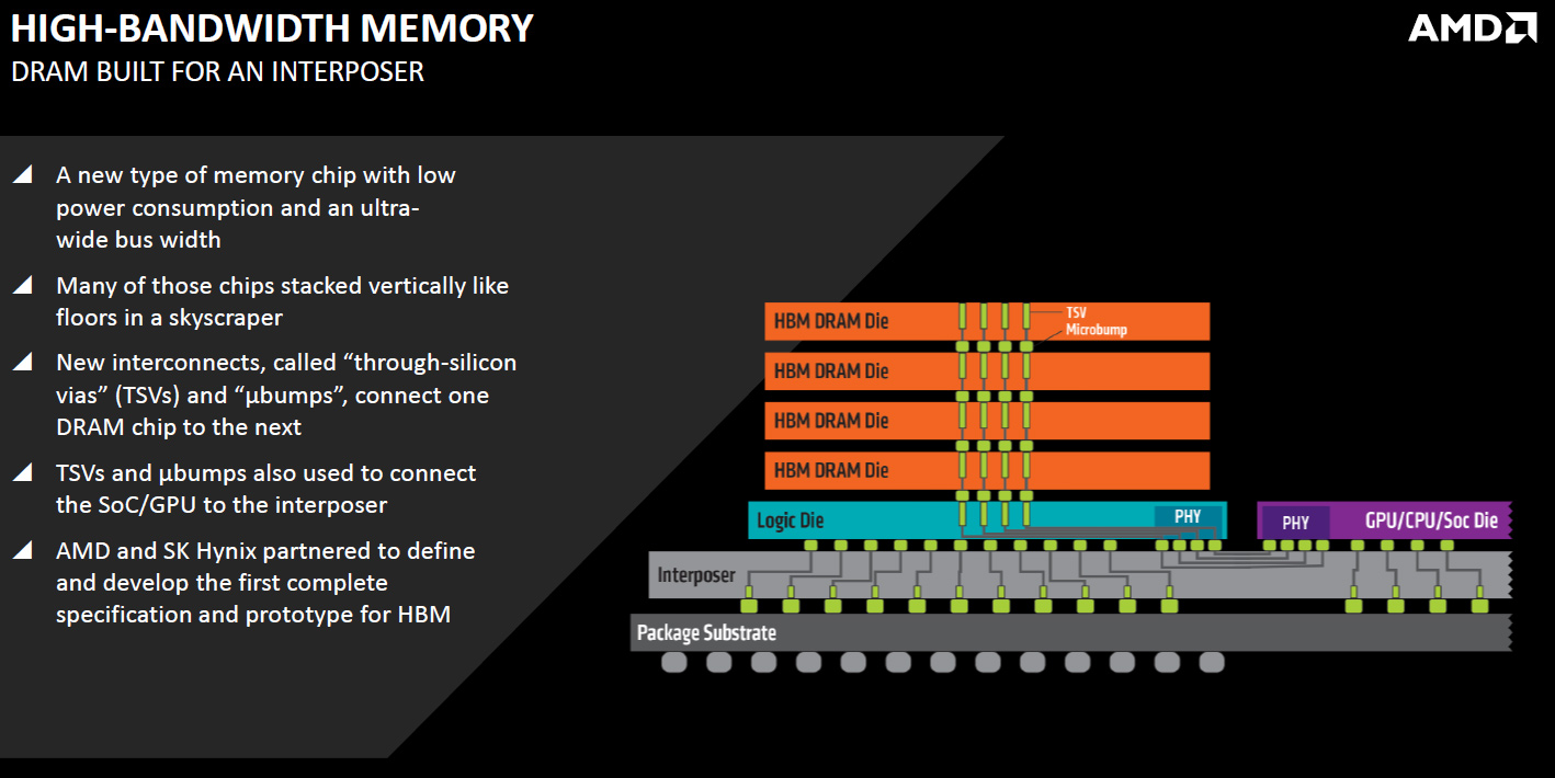
There are several key technologies that empower HBM:
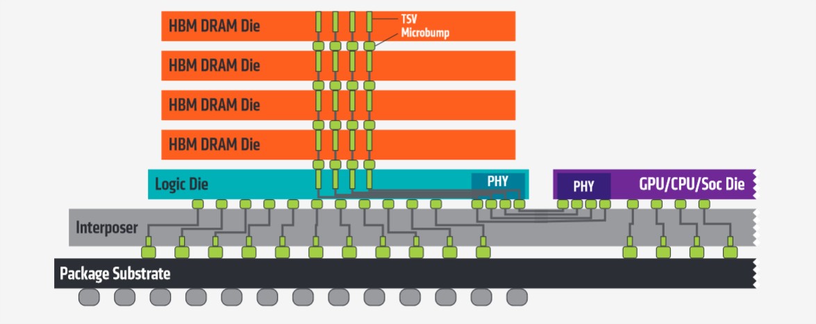
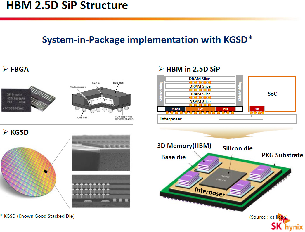
- Memory chips with multiple vertically stacked memory devices interconnected using through-silicon-vias (TSVs) and microbumps and then placed on a base logic die.
- Silicon interposer that connects memory ICs to host processor using an ultra-wide interface. Silicon interposer is made using a photolithography technology in a semiconductor fabrication plant.
- Host processor with ultra-wide memory interface.
Development of new technologies requires a lot of prototyping activities in general. Before AMD and SK Hynix proceeded to standardize their HBM memory with JEDEC in 2010, the companies had to design multiple implementations of their new technologies and learn how they operated in real-life.
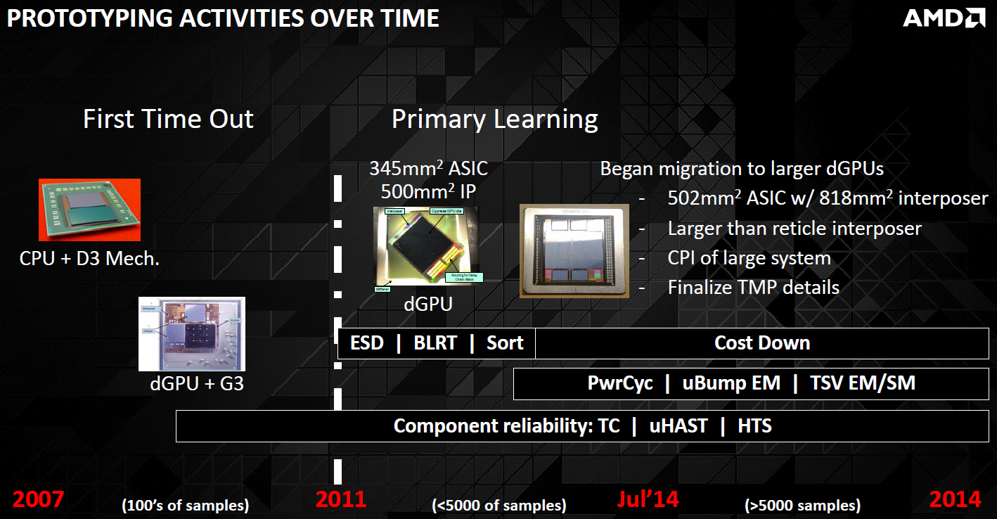
AMD started to experiment with interposers and processors back in 2007. The first GPU to connect to memory using an interposer was the RV635, which powered ATI Radeon HD 3650/3670 graphics adapters. Eventually, AMD experimented with interposers and the “Cypress”, which was the world’s first DirectX 11-supporting graphics processor. Both the RV635 and the “Cypress” were based on the TeraScale architecture (gen 1 and gen 2), which was succeeded by the GCN [graphics core next] architecture in 2012.
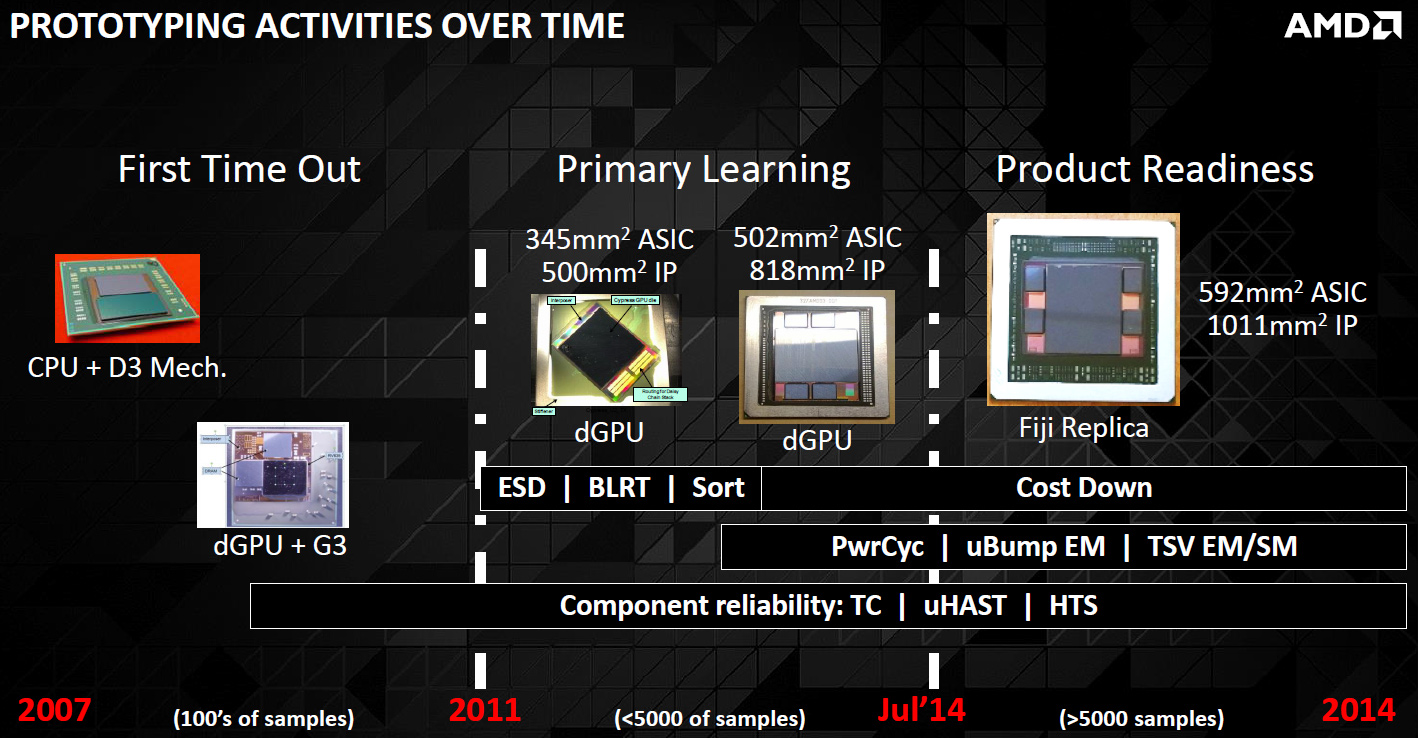
The JESD235 standard was published in October, 2013, when the work on AMD’s “Fiji” was well underway and the graphics processing unit was months away from tape-out.
The HBM saga continues
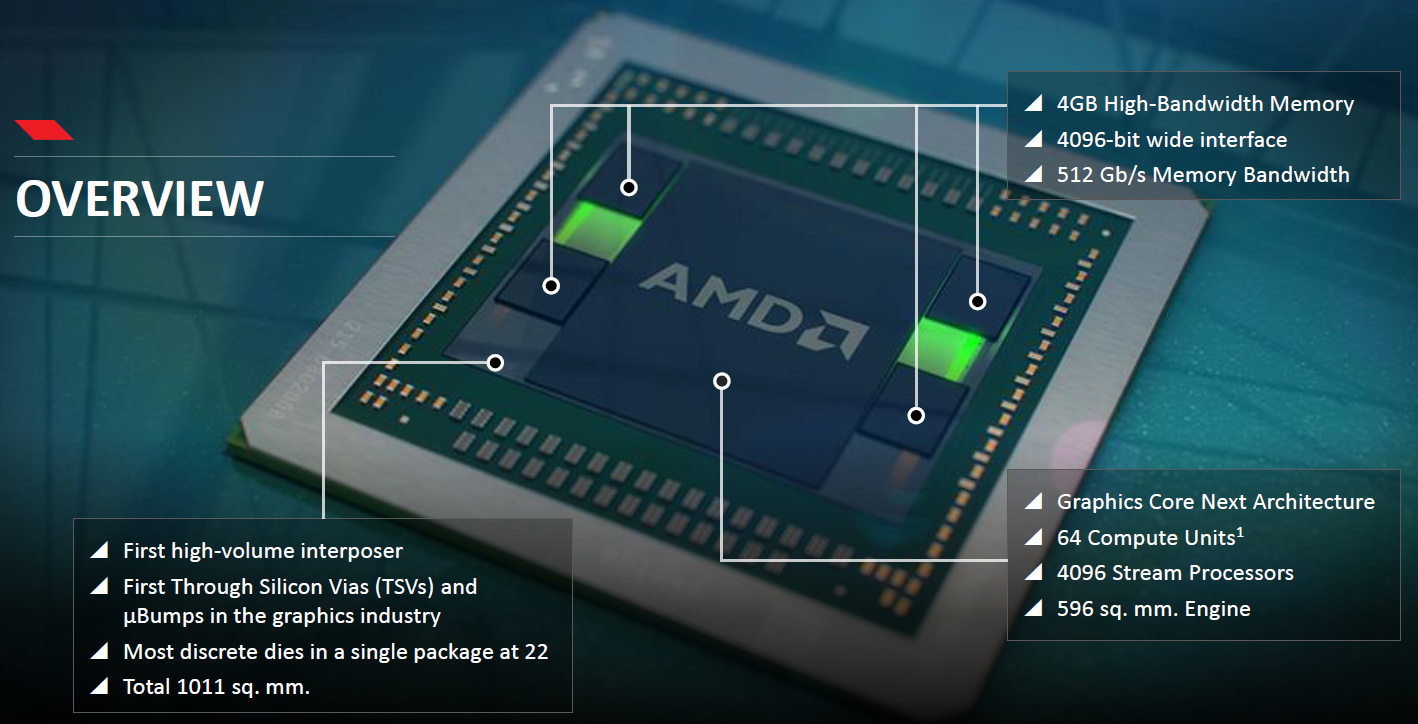
The first-generation HBM (HBM1) stacks four DRAM dies with two independent 128-bit channels per die on a base logic die, creating a memory device with a 1024-bit interface. Each channel supports 1Gb capacities (2Gb per die), features 8 banks and can operate at 1Gb/s data-rate (1GHz effective DDR clock-rate). As a result, each HBM 4Hi stack (4 high stack) package can provide 1GB capacity and 128GB/s memory bandwidth. AMD’s Radeon R9 Fury X flagship graphics adapter features 4GB of HBM memory with unprecedented bandwidth of 512GB/s. While the first-gen HBM has limitations when it comes to capacity, it allows to create very small and very high performance graphics solutions thanks to the fact that HBM chips are smaller than GDDR5 ICs.
The second-generation HBM (HBM2) utilizes 8Gb dies with two 128-bit channels featuring 16 banks and sporting up to 2Gb/s data-rates (2GHz effective DDR frequency). The architecture of the HBM2 will let manufacturers built not only 4Hi stack (4 high stack) packages, but also 2Hi stack and 8Hi stack devices. As a result, memory producers will be able to assemble HBM2 memory chips with up to 8GB capacity (8Hi stack) and up to 256GB/s bandwidth (2Gb/s data rate, 1024-bit bus).

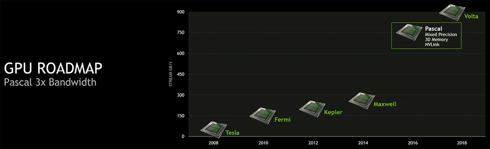
Architectural advantages of HBM2 will allow GPU developers to use it not only for ultra-high-end applications with 4096-bit memory bus, but also for adapters that do not require extreme performance. Next-generation enthusiast-class graphics cards based on AMD’s “Greenland” graphics processors as well as Nvidia’s GP100 (“Pascal”) GPUs will feature 8GB – 16GB of HBM memory with up to 1TB/s bandwidth. Samsung Electronics forecasts that over time HBM will enable add-in-boards with up to 48GB of memory.
The third-generation HBM is in development and engineers currently do not share any information about it. It is logical to expect further increases of capacities as well as performance. While we have no idea how additional capacities and performance will be achieved, we are pretty sure that engineers at companies like AMD are already playing not only with prototypes of future implementations of HBM, but also with something that will succeed them a long time down the road.
http://www.kitguru.net/components/gr...-a-decade-ago/
Teremos de aguardar mais algum tempo até vermos o que esta nova memória nos vai trazer, sendo que ainda está numa primeira geração.
-
04-09-15, 14:04 #8Tech Ubër-Dominus
- Registo
- Nov 2013
- Local
- City 17
- Posts
- 30,121
- Likes (Dados)
- 0
- Likes (Recebidos)
- 2
- Avaliação
- 1 (100%)
- Mentioned
- 0 Post(s)
- Tagged
- 0 Thread(s)
AMD: We are actively promoting HBM and do not collect royalties
Noticia:Advanced Micro Devices is currently the only company to use high-bandwidth memory it co-developed with SK Hynix and other partners. While usage of HBM is clearly a competitive advantage that AMD has over its rivals, the company is encouraging others to use the new memory type and does not intend to collect any royalties for HBM.
It has taken AMD over 8.5 years to develop high-bandwidth memory and a set of technologies that enable new DRAM chips as well as their interface with host processors. In a bid to make HBM memory more affordable, more developers of graphics processors and other bandwidth-demanding chips have to use this technology. Once HBM gets less expensive than today, the industry in general will benefit from this.

Nvidia Corp. has publicly revealed that its next-generation “Pascal” architecture of graphics processors supports second-generation HBM memory and in 2016 graphics cards with GP100 GPUs and HBM2 DRAM will hit the market. In fact, HBM support is a key feature of Nvidia’s “Pascal”, which will help the company to triple the bandwidth available to its next-gen GPUs, thus significantly improving their performance.
Earlier this week a web-site reported that Nvidia will delay adoption of HBM because of royalties demanded by AMD for its HBM-related intellectual property. In particular, it is reported that 2.5D GPU packaging used for the “Fiji” graphics processing unit is covered by AMD’s patents and Nvidia either needs to design its own package or pay licensing fees to its rival. According to AMD, this is not true.
“AMD is not involved in collecting any royalties for HBM,” said Iain Bristow, a spokesman for AMD. “We are actively encouraging widespread adoption of all HBM associated technology on [Radeon R9] Fury products and there is no IP licensing associated.”
Advanced Micro Devices owns a number of patents covering HBM, but as that intellectual property is a part of JEDEC’s JESD235 standard, it has to be licensed to applicants desiring to implement the standard “either without compensation or under reasonable terms and conditions that are free of any unfair discrimination.”

Nvidia did not comment on the news-story.
http://www.kitguru.net/components/gr...ect-royalties/
-
04-09-15, 16:54 #9Tech Membro

- Registo
- Mar 2013
- Local
- C.Branco
- Posts
- 2,326
- Likes (Dados)
- 0
- Likes (Recebidos)
- 0
- Avaliação
- 0
- Mentioned
- 0 Post(s)
- Tagged
- 0 Thread(s)
Por um lado, neste mundo de "scumbags", patentes, e capitalistas, talvez a AMD faça mal em não tentar arrecadar o máximo de guito através disso, que bem precisa.
Mas tendo em conta a sua actual percentagem de mercado, seria pouco produtivo tentar fechar ao máximo algo que os beneficia mais a eles, e que precisam que seja standard para colher esses frutos em pé de igualdade... tal como o caso do Mantle/DX12/Vulkan. Quanto mais depressa vierem jogos DX12 com aproveitamento das specs que a AMD tem vindo a apostar, melhor. Problema será fazer frente depois ao abastado departamento de R&D da nVidia, que nesta altura deve andar em passo acelerado para se colocar bem à frente da própria rival em tech HBM. Poderá ser um rude golpe para a AMD se a vantagem e experiência não se revelar suficiente.
-
17-11-15, 13:50 #10Tech Ubër-Dominus
- Registo
- Nov 2013
- Local
- City 17
- Posts
- 30,121
- Likes (Dados)
- 0
- Likes (Recebidos)
- 2
- Avaliação
- 1 (100%)
- Mentioned
- 0 Post(s)
- Tagged
- 0 Thread(s)
Intel and Altera Develop World’s First HBM2, 2.5D Stacked, SiPs With Integrated Stratix 10 FPGA and SoC Solution
HBM2 is quickly shaping up to be the future of next generation graphic cards and of very critical importance to both GPU manufacturers. Altera (now a subsidiary of Intel) has recently launched the world’s first System-in-Package (SIP) device which consists of HBM2 DRAM combined with FPGAs. As many of our readers will know, the logic of an FPGA can be reprogrammed which allows it unparalleled flexibility in certain computing tasks – a capability, which, when combined with HBM2 technology could result in astonishing results.

Altera introduces world’s first Stratix 10 FPGA SiP device with HBM2 (memory)
FPGAs stand for Field Programmable Gate Arrays. For those not familiar with them, they are a type of processing device that has reconfigurable logic. Basically, you have ASICs which have hard-wired logic, tailored to a specific task and a specific load type allowing them to accomplish said tasks with unparalleled efficiency. Then, you have our modern day CPUs with hard-wired logic that allows many general applications and diverse load types resulting in an all rounder processor capable of doing just about everything – but not very good at certain load types. And finally, you have FPGAs, whose logic is not hard-wired and can be reconfigured accordingly resulting in a very customizable silicon solution for the semi-custom market.

The technology will use Altera’s Stratix chips (SoCs and FPGAs) and combine them with Intel’s EMIB fabric. The result is a device that can handle some specific work loads exceptionally well. Whether this will have any impact in the graphics segment of the industry – is anyone’s guess. But even if it does, it will most probably be limited to professional GPUs and not the mainstream ones that most PC users are interested in. Altera had the following to say at the time of launch:
“Supporting higher memory bandwidth requirements is one of the biggest challenges many of our customers face as they implement more computationally intensive tasks in their systems, such as machine learning, big data analytics, image recognition, workload acceleration and 8K video processing,” said Danny Biran, senior vice president of corporate strategy and marketing at Altera. “Altera is in a unique position to serve these system requirements by combining the industry’s highest performance FPGA with High-Bandwidth Memory in a single package. No other programmable solution can match Stratix 10 DRAM SiP in terms of performance, power efficiency and memory bandwidth.”It is worth noting at this point, that AMD has already patented a technology along the very same lines some while ago – which means, that this is something that the Industry has been working on for quite a long time and is just recently becoming public (as is usually the case). What benefit these will net the average user is something that is of considerable mystery right now. The Zen-FPGA-HBM design does make sense but the patent published was a very general one and we have not heard anything about it actually being pursued. Intel and Altera however are already pursuing clients in the high performance compute sector and guiding them about integration of the Stratix 10 SiP HBM2 device. It is expected to ship sometime in the 2016-2017 time frame.
-
12-01-16, 15:47 #11Tech Ubër-Dominus
- Registo
- Nov 2013
- Local
- City 17
- Posts
- 30,121
- Likes (Dados)
- 0
- Likes (Recebidos)
- 2
- Avaliação
- 1 (100%)
- Mentioned
- 0 Post(s)
- Tagged
- 0 Thread(s)
JEDEC Updates Groundbreaking High Bandwidth Memory (HBM) Standard
Noticia:JEDEC Solid State Technology Association, the global leader in the development of standards for the microelectronics industry, today announced the publication of an update to JESD235 High Bandwidth Memory (HBM) DRAM standard. HBM DRAM is used in Graphics, High Performance Computing, Server, Networking and Client applications where peak bandwidth, bandwidth per watt, and capacity per area are valued metrics to a solution's success in the market. The standard was developed and updated with support from leading GPU and CPU developers to extend the system bandwidth growth curve beyond levels supported by traditional discrete packaged memory. JESD235A is available for free download from the JEDEC website.
JESD235A leverages Wide I/O and TSV technologies to support up to 8 GB per device at speeds up to 256 GB/s. This bandwidth is delivered across a 1024-bit wide device interface that is divided into 8 independent channels on each DRAM stack. The standard supports 2-high, 4-high and 8-high TSV stacks of DRAM at full bandwidth to allow systems flexibility on capacity requirements from 1 GB - 8 GB per stack.
Additional improvements in the recent update include a new pseudo channel architecture to improve effective bandwidth, and clarifications and enhancements to the test features. JESD235A also defines a new feature to alert controllers when DRAM temperatures have exceeded a level considered acceptable for reliable operation so that the controller can take appropriate steps to return the system to normal operation.
"GPUs and CPUs continue to drive demand for more memory bandwidth and capacity, amid increasing display resolutions and the growth in computing datasets. HBM provides a compelling solution to reduce the IO power and memory footprint for our most demanding applications," said Barry Wagner, JEDEC HBM Task Group Chairman.
http://www.techpowerup.com/219175/je...-standard.html
-
19-01-16, 09:32 #12Tech Ubër-Dominus
- Registo
- Nov 2013
- Local
- City 17
- Posts
- 30,121
- Likes (Dados)
- 0
- Likes (Recebidos)
- 2
- Avaliação
- 1 (100%)
- Mentioned
- 0 Post(s)
- Tagged
- 0 Thread(s)
Samsung announces mass production of 4GB HBM2-based DRAM chips
Noticia:Samsung has just announced that it has entered mass production of 4GB DRAM on the HBM2 interface, which will be used for "high performance computing (HPC), advanced graphics and network systems, as well as enterprise servers".

The new 4GB HBM2-based DRAM uses Samsung's 20nm process, and "advanced HBM chip design", which "satisfies the need for high performance, energy efficiency, reliability and small dimensions making it well suited for next-generation HPC systems and video cards". The new 4GB HBM2 DRAM is created by stacking a buffer die at the bottom and four 8-gigabit core dies on top. From there, they're vertically interconnected by TSV holes and microbumps, with a single 8Gb HBM2 die featuring over 5000 TSV holes, which is more than 36x that of a 8Gb TSV DDR4 die.
Bandwidth wise, Samsung's new HBM2-based DRAM package features 256Gbps of bandwidth, double that of HBM1. This is a huge 7x increase over the piddly 36Gbps bandwidth that a 4Gb GDDR5 DRAM chip features. Samsung's new 4GB HBM2 DRAM is also much more power efficient, featuring 2x the bandwidth-per-watt over a 4Gb GDDR5-based solution.
http://www.tweaktown.com/news/49760/...ips/index.html
Assim não há desculpas para existirem atrasos para quem vai utilizar isto nas placas graficas.
-
16-02-16, 09:14 #13Tech Ubër-Dominus
- Registo
- Nov 2013
- Local
- City 17
- Posts
- 30,121
- Likes (Dados)
- 0
- Likes (Recebidos)
- 2
- Avaliação
- 1 (100%)
- Mentioned
- 0 Post(s)
- Tagged
- 0 Thread(s)
Samsung's HBM2 will be ready before you are
Noticia:Samsung is ready to roll out the next generation of High Bandwidth Memory, aka HBM2, for your desktop and not just your next generation of GPU. They have already begun production on 4GB HBM2 DRAM and promise 8GB DIMMs by the end of this year. The modules will provide double the bandwidth of HBM1, up 256GB/s of bandwidth which is very impressive compared to the up to 70GB/s DDR4-3200 theoretically offers.
Not only is this technology going to appear in the next genertation of NVIDIA and AMD GPUs but could also work its way into main system memory. Of course these DIMMs are not going to work with any desktop or mobile processor currently on the market but we will hopefully see new processors with compatible memory controllers in the near future. You can also expect this to come with a cost, not just in expensive DIMMs at launch but also a comparible increaset in CPU prices as they will cost more to manufacture initially.
It will be very interesting to see how this effects the overall market; will we see a split similar to what is currently seen in mainstream GPUs, a lower cost DDR version and a standard GDDR version? The new market could see DDRx and HMBx models of CPUs and motherboards and could do the same for the GPU market, with the end of DDR on graphics cards. If so will it spell the end of DDR5 development? Interesting times to be living in, we should be hearing more from Samsung in the near future.

You can read the full PR below.
Samsung Kick-Starts Next Generation of Memory with High Bandwidth Memory DRAM
Market leading Samsung has started the race to bring the next generation of RAM memory to market, with the innovative High Bandwidth Memory (HBM2) DRAM now coming out of its factories.
The new DRAM is being heralded as the ‘latest and greatest’, and will offer twice the bandwidth of the old HBM1 memory. Users will get data in and out at 256GBps, and there will be various capacities available. Though the memory modules have already gone into production, the Korean manufacturer isn’t saying when the industry-first 4GB DRAM modules will hit the shelves – but they have guaranteed an 8GB version before the end of 2016.
Data Memory Systems, one of the US’ leading providers of computer memory solutions, is renowned for keeping its finger on the pulse of all the latest goings-on in the world of tech. The experts at the firm are looking forward to welcoming the next generation of DRAM to their stock.
A spokesman for Data Memory Systems says, “Technology moves faster than ever nowadays, and we’re always poised for the latest developments and breakthroughs. This announcement by Samsung marks the beginning of next-generation DRAM, with speeds up to seven times faster than its predecessors.”
The spokesman adds, “The memory has only just been put into production and will likely become available over the course of the next year – we eagerly anticipate being able to sell these modules on our site, which is renowned for being one of the US’ premier memory suppliers for business and individuals alike.”
The new DRAM has been produced with an eye on high-performing computing, advanced graphics and network systems, and enterprise services. According to Samsung themselves, the rapid adoption of high-performance computing systems by IT companies across the globe was the key factor in them deciding to produce a memory module that’s suitable for the demands of these systems.
The new modules will also be effective for those who seek components for high-end gaming computers. The DRAM will enable graphics-intensive applications to run flawlessly, which will be ideal for the die-hard PC gamers out there that don’t want to compromise when it comes to their tech.
A further announcement from Samsung on the HBM DRAM modules is anticipated over the coming months. Until then, those seeking a computer memory upgrade will find a multitude of options at Data Memory Systems, from external hard drives to RAM modules for any device.
http://www.pcper.com/news/Memory/Sam...-ready-you-are
Cá esperamos por ela e para ver o que é capaz de dar aos novos GPUs.
-
16-02-16, 20:17 #14Master Business & GPU Man
- Registo
- Jan 2015
- Local
- País Campeão Euro 2016
- Posts
- 7,793
- Likes (Dados)
- 0
- Likes (Recebidos)
- 1
- Avaliação
- 41 (100%)
- Mentioned
- 0 Post(s)
- Tagged
- 0 Thread(s)
Pois...mas o que eles falam aqui mais em concreto e como novidade, é substituirem as DDR4 dos desktops. Post Original de Jorge-Vieira
 Ideias sem Nexo e Provas do Tráfico de Hardware
"que personifica o destino, equilíbrio e vingança divina." Dejá vú. Que cena!
-
07-03-16, 21:18 #15Tech Ubër-Dominus
- Registo
- Nov 2013
- Local
- City 17
- Posts
- 30,121
- Likes (Dados)
- 0
- Likes (Recebidos)
- 2
- Avaliação
- 1 (100%)
- Mentioned
- 0 Post(s)
- Tagged
- 0 Thread(s)
SK Hynix To Commence Mass Production of 4 GB HBM2 DRAM In Q3 2016 – Aiming at NVIDIA Pascal and AMD Polaris GPUs
SK Hynix is planning to commence production of their HBM2 DRAMs in Q3 2016, as reported by Golem.de. The source reveals that SK Hynix will be initiating full fledged mass production of 4 GB HBM2 DRAMs in Q3 ’16 and followed quickly with 8 GB HBM2 DRAMs in Q4 ’16. SK Hynix will be aiming to supply NVIDIA’s Pascal and AMD Polaris GPUs, both of which are expected to arrive in mid of 2016.

SK Hynix To Commence 4 GB HBM2 DRAM Die Production in Q3 2016, 8 GB DRAM Dies in Q4 2016
SK Hynix seems to be aiming a steady pace for their HBM2 DRAM production. Just like Samsung who went with 4 GB HBM2 dies first, SK Hynix will be choosing a similar path with mass production commencing in Q3 2016. It does make SK Hynix a little late knowing that Samsung has had their production initiated while 8 GB HBM2 dies are planned for this year too, although no specific date is given yet.
SK Hynix shipped the very first HBM dies with AMD’s Radeon R9 Fury series cards last year. AMD was the very first GPU company to incorporate the first generation of high bandwidth memory standard on their cards and this year will see an even greater influx of HBM powered graphics cards from both NVIDIA and AMD. Samsung already has mass production started but SK Hynix is planning to get production started in Q3 2016 which gives them time to see the market trends for high-performance and mid-range GPUs.
In the interview with Golem.de, an SK Hynix representative stated that the company will be begin HBM2 DRAM production in second half of 2016 (Q3 2016 to be precise). The HBM2 DRAM from SK Hynix will be offered as an alternative to Samsung’s HBM2 stack, hence being used on both AMD’s 14nm FinFET based Polaris GPUs and NVIDIA’s 16nm FinFET based Pascal GPUs.
Image Credits: Golem.deThe new HBM2 memory makes use of beefier 8Gb (Gigabit) dies which are connected and stacked vertically through the TSVs. Each package of these dies is able to deliver speeds of 256 GB/s (Gbps bandwidth) which is twice the bandwidth of current generation HBM1 memory that provides a 128 GB/s bandwidth and over 7x increase compared to a 4 Gb GDDR5 DRAM chip (36 Gbps). The 4 GB HBM2 package can be incorporated in several stacks, offering higher memory space at better efficiency than current generation DRAM solutions. Having either two of these packages on an interposer would get 8 GB of VRAM along with 512 GB/s of total bandwidth and four packages would mean 16 GB of VRAM and 1 TB/s bandwidth.
Advertisements
HBM is a leading edge memory solution which was first adopted by high-end graphics cards. It is known to have provided the best solutions possible through implementation of 3D, 4K display, Virtual Reality and other upgraded functions.
The usage of HPC(High-performance computing) has extended to various applications in the purpose of processing and storing huge amounts of big data. A high density memory using TSV stacking technology, HBM answers calls for cost-effective memory solutions, securing its reputation as “the most effective” memory for HPC and related products.
In other words, HBM, which has advantages in high performance, low power and small form factor, will help overcome DRAM maximum speed and density limitations which will result in the explosive expansion of HBM demand. via SK Hynix
A quad stack of 4-Hi HBM2 stacks with 4 GB dies will give 16 GB VRAM, you increase the density of the DRAM to 8 GB and you’ll be getting 32 GB VRAM off the same layout. HBM2 is very scalable in nature allowing range of SKUs compared to HBM1. You cannot just have different stacks and layouts but HBM2 also allows each die to run at a specific speed to conserve power. All HBM2 dies from SK Hynix will run at 2.0 Gbps but can also be lowered down to 1.6 Gbps and 1.0 Gbps speeds. It all depends on the application and usage of the solution.
It will be interesting to see if cards aside from high-end, enthusiast grade stuff get to use HBM2. Micron’s GDDR5X solution is set to be seen on several graphics cards which we speculated about in detail in our previous article. Samsung sure has the edge when it comes to HBM2 production since they started earlier, SK Hynix will be shipping their first samples in Q3 2016 while Samsung is expected to mass produce 8 GB HBM2 dies by then. Nevertheless, 2016 seems to be a great year for memory makers as higher bandwidth solutions remain in the spot light.
GDDR5 vs HBM Comparison:
DRAM GDDR5 HBM1 HBM2 I/O (Bus Interface) 32 1024 1024 Prefetch (I/O) 8 2 2 Maximum Bandwidth 32GB/s
(8Gbps per pin)128GB/s
(1Gbps per pin)256GB/s
(2Gbps per pin)tRC 40ns(=1.5V)
48ns(=1.35V)48ns 45ns tCCD 2ns (=4tCK) 2ns (=1tCK) 2ns (=1tCK) VPP Internal VPP External VPP External VPP VDD 1.5V, 1.35V 1.2V 1.2V Command Input Single Command Dual Command Dual Command


 Responder com Citação


Informação da Thread
Users Browsing this Thread
Estão neste momento 1 users a ver esta thread. (0 membros e 1 visitantes)
 Regras
São agora 23:32.
 User Alert System provided by
Advanced User Tagging v3.3.0 (Lite) -
vBulletin Mods & Addons Copyright © 2024 DragonByte Technologies Ltd.
User Alert System provided by
Advanced User Tagging v3.3.0 (Lite) -
vBulletin Mods & Addons Copyright © 2024 DragonByte Technologies Ltd.
Feedback Buttons provided by Advanced Post Thanks / Like (Lite) - vBulletin Mods & Addons Copyright © 2024 DragonByte Technologies Ltd.
Portugal-Tech 2012-24 | Todos os direitos reservados! Alojamento Powered by: Trignosfera
Powered by vBulletin® Version 4.2.5 Alpha 3
Copyright © 2024 vBulletin Solutions, Inc. All rights reserved.
Copyright © 2024 vBulletin Solutions, Inc. All rights reserved.
Feedback Buttons provided by Advanced Post Thanks / Like (Lite) - vBulletin Mods & Addons Copyright © 2024 DragonByte Technologies Ltd.
Portugal-Tech 2012-24 | Todos os direitos reservados! Alojamento Powered by: Trignosfera
Bookmarks