Introduction
DirectX 10 is sitting just around the corner, hand in hand with Microsoft Vista. It requires a new unified architecture in the GPU department that neither hardware vendor has implemented yet and is not compatible with DX9 hardware. The NVIDIA G80 architecture, now known as the GeForce 8800 GTX and 8800 GTS, has been the known DX10 candidate for some time, but much of the rumors and information about the chip were just plain wrong, as we can now officially tell you today.
Come find out why the GeForce 8800 GTX should be your next GPU purchase.
What is a Unified Architecture?
The requirement of a unified architecture is one of the key changes to the upcoming release of DirectX 10 on Windows Vista. The benefits and pitfalls of a unified graphics architecture have been hotly debated since DX10 specs first became known several years ago. With Vista just months away now, both NVIDIA and ATI no longer get to debate on the logic of the move; now they have to execute on it.
A unified graphics architecture, in its most basic explanation, is one that does away with seperate pixel pipelines and texture pipelines in favor of a single "type" of pipeline that can be used for both.
 Traditional GPU Architecture and Flow
 This diagram shows what has become the common GPU architecture flow; starting with vertex processing and ending with memory access and placement. In G70, and all recent NVIDIA and ATI architectures, there was a pattern that was closely followed to allow data to become graphics on your monitor. First, the vertex engine, starting out and pure texture and lighting hardware, processing the vertex data into cohesive units and passes it on to the triangle setup engine. Pixel pipes would then take the data and apply shading and texturing and pass the results onto the ROPs that are responsible for culling the data, anti-aliasing it (in recent years) and passing it in the frame buffer for drawing on to your screen.
This scheme worked fine, and was still going strong with DX9 but as game programming became more complex, the hardware was becoming more inefficient and chip designers basically had to "guess" what was going to be more important in future games, pixel or vertex processing, and design their hardware accordingly.

A unified architecture simplifies the pipeline significantly by allowing a single floating point processor (known as a pixel pipe or texture pipe before) to work on both pixel and vertex data, as well as new types of data such as geometry, physics and more. These floating point CPUs then pass the data onto a traditional ROP system and memory frame buffer for output that we have become familiar with.

I mentioned above that because of the inefficiencies of the two-pipeline-style, hardware vendors had to "guess" which type was going to be more important. This example showcases this point very well: in the top scenario, the scene is very vertex shader heavy while the pixel shaders are being under utilized, leaving idle hardware. In the bottom scenario, the reverse is happening, as the scene is very pixel shader intensive leaving the vertex shaders sitting idle.
Any hardware designer will tell you that having idle hardware when there is still work to be done is perhaps the single most important issue to address. Idle hardware costs money, it costs power and it costs efficiency -- all in the negative direction. Unified shaders help to prevent this curse on computing hardware.

In the first example, notice that the sample "GPU" had 4 sets of vertex shaders and 8 sets of pixel shaders; a total of 12 processing units that were used inefficiently. Here we have another GPU running with 12 unified processing shaders that can dynamically be allocated to work on vertex of pixel data as the scene demands. In this case, in the top scene that was geometry heavy uses 11 of the 12 shaders for vertex work and 1 for pixel shading, using all 12 shaders to their maximum potential.
This is of course the perfect, theoretical idea behind unified architectures, and in the real world the problem is much more complex.

In the real world, there are more than 12 processor pipelines and the ability to break down a scene into "weights" like we did above is incredibly complex. NVIDIA's new G80 hardware has the ability to dynamically load balance in order to get as high of an efficiency out of the unified shaders as possible. As an example from Company of Heroes, on the left is a scene with little geometry and one on the right with much more geometry to process. The graph at the bottom here shows a total percentage usage of the GPU, yellow representing pixel shading work and red representing vertex shading work. When the scene shifts from the left to the right view, you can see that the amount of vertex work increases dramatically, but the total GPU power being used remains the same; the GPU has load balanced the available processing queue accordingly.
DirectX 10
So the move to unified shaders is a requirement of DX10 as I mentioned before, but that's not all that has changed in the move to double-digits. The goal from Microsoft's DX10 designers was mainly to improve the ease of programming and allow the designers to more easily implement improved graphics, effects and more. Shader Model 4.0 is being introduced with some big enhancements and geometry shaders make their debut as well. Another important note about DX10 is that it is much more strict on the hardware specifications -- with no more "cap bits" hardware vendors can't simply disable some DX10 features to qualify as DX10 hardware, as Intel did in many cases with DX9.

The updated DX10 pipeline looks a little something like this; new features are listed off to the right there. Geometry shaders and stream output are two very important additions to the specification. Geometry shaders will allow dynamic modifications of objects in the GPU (rather than the CPU) and will give game creators a boost in creativity. Stream output allows the processing engine (GPU) that DX10 runs on to communicate within the GPU, effectively allowing the pipelines to communicate with each other by outputting to shared memory.
The geometry shader is placed right after the vertex shader in the DX10 pipeline, allow the vertex data to setup the geomerty that may be modified by the new processing unit. The input and output from the geometry shaders must follow the same basic types as points, lines or triangle strips, but the data has the possibility of being modified inside the shader to produce various effects.
Here are some examples of what designers might be able to do with geometry shaders; automatic shadow box generation and physical simulations are among the most powerful. Real-time environment creation is a fantastic idea that could allow a game's replay value to be potentially limitless; imagine games where the world really DOESN'T end can be dynamically generated on the fly by the gamer's GPUs to be different than any other gamer's.

Stream output is the other new addition to the DX10 pipeline and its importance will be seen in great detail through out this review and in the future months as more about NVIDIA's processing potential is revealed. Strictly for gaming, stream output allows for a mid-phase memory write by the processing engine to store geometry or vertex shader data. By enabling multi-pass operations, programmers can now do recursion (the bane of my undergraduate years...) as well as numerous other "tricks" to improve their software.
Maybe you remember a thing called physics? It's all the rage in gaming recently, and with the ability to output data to memory mid-phase in the processing pipeline, NVIDIA is going to be able to compete with AGEIA's hardware more directly as that ability to communicate between pipes is what gave AGEIA's PhysX engine a performance advantage.

Another example of stream output at work is improved instancing -- where before you were limited to instancing items like grass that would all look the same and following the same paths, with stream output you can have instanced items that have individual "states" and attirbutes that allow programmers to use them for unique characters and items.
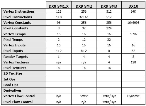
For data junkies, this table summarizes up the changes moving from DX8 and Shader Model 1.0 to DX10 and the new SM4.0 specs.
All of this new DX10 ability will allow programmers to do more than ever on the GPU, removing the CPU as a gaming bottleneck in many cases. Here are a couple of examples: above we see an algorithm for human hair simulation. Before, the majority of the physics and setup work was done on the CPU but now with the new options DX10 provides it can all be moved to the GPU.
Another example is using a stencil shadow algorithm (a popular method in current games) where most of the work previously relegated to the CPU can be moved to the GPU using DX10.
As an example of DX10 at work, this NVIDIA demo shows a landscape being created on the fly using geometry shaders with a particle system running only on the GPU to simulate the water running down the rock. Oh, and the graphics are rendered on it too.
The G80 Architecture
Well, we've talked about what a unified architecture is and how Microsoft is using it in DX10 with all the new features and options available to game designers. But just what does NVIDIA's unified G80 architecture look like??
 Click to Enlarge
All hail G80!! Well, um, okay. That's a lot of pretty colors and boxes and lines and what not, but what does it all mean, and what has changed from the past? First, compared to the architecture of the G71 (GeForce 7900), which you can reference a
block diagram of here, you'll notice that there is one less "layer" of units to see and understand. Since we are moving from a dual-pipe architecture to a unified one, this makes sense. Those eight blocks of processing units there with the green and blue squares represent the unified architecture and work on pixel, vertex and geometry shading.
Even the setup events at the top of the design are completely new, from the Host and below. The top layer of the architecture that includes the "Vtx Thread issue, Geom Thread Issue and Pixel Thread Issue" units is part of the new thread processor and is responsible for maintaining the states of the numerous processing threads that are active at one time and assigning them to (or issuing) processing units as they are needed. With this many processing units and this many threads, this unit is going to keep quite busy...

Okay, so how many are there already?? There are 128 streaming processors that run at 1.35 GHz accepting dual issue MAD+MUL operations. These SPs (streaming processorss) are fully decoupled from the rest of the GPU design, are fully unified and offer exceptional branching performance (hmm...). The 1.35 GHz clock rate is independent of the rest of the GPU, though all 128 of the SPs are based off of the same 1.35 GHz clock generator; in fact you can even modify the clock rate on the SPs seperately from that of the GPU in the overclocking control panel! The new scalar architecture on the SPs benefits longer shader applicaitons to be more efficient when compared to the vector architecture of the G70 and all previous NVIDIA designs.
The L1 cache shown in the diagram is shared between 16 SPs in each block, essentially allowing these 16 units to communicate with each other in the stream output manner we discussed in the DX10 section.

Looking at the raw numbers, you can see that the GeForce 8800 SP architecture creates some impressive processing power, resulting in more than double the "multiplies" that the G71 or R580 could muster. Also, we found out that the new G80 SPs are 1 to 2 orders of magnitude faster than G71 was on branching -- this should scare ATI as their branching power was one of the reasons their R580 architecture was able to hold off the 7900 series for as long as it did.

In previous generations of NVIDIA's hardware, the texture units actually used a small portion of the pixel shader in order to keep from doubling up on some hardware. This has the potential to create "bubbles" in the GPU processing that looked like the GeForce 7-series diagram above. Math operations often had to wait for texture units to complete their work before continuing. That is no longer the case with G80; there are literally thousands of threads in flight at any given time allowing the memory access to completely decouple from processing work. This keeps those "bubbles" from occuring in this new design allowing for seemingly faster memory access times.
This threading process has been dubbed "GigaThreading" by NVIDIA and refers to the extremely high amout of active threads at any given time. In a CPU, when a cache miss occurs, the CPU usually has to wait for that data to be retrieved and the thread stalls as it waits. On the G80, if there is a data cache miss, the problem isn't so severe as there are many threads ready to be placed into one of the 128 SPs while the data is retrieved for the cache miss. And in case you were wondering what this constant thread swapping might add to computing overhead, NVIDIA told us that it technically takes 0 clocks for threads to swap!

Moving on to the texture units on the G80, there are two texture fetch (TF) units for every texture address (TA) unit; this allows for a total of 32 pixels per clock of texture addressing and 64 pixels per clock of texture filter ops. These units have been optimized for HDR processing and work in full FP32-bit specifications, but can support FP16 as well. Because of all this power, the G80 can essentially get 2x anisotropic filtering for free, as well as FP16 HDR for free.
This small table compares the 7900 GTX, X1950 XTX and the 8800 GTX in terms of texture fill rates; on 32-bit dual texturing, the X1950 XTX and the 7900 GTX could get approximately 50% performance on 2x AF while the 8800 GTX gets 100% performance because and 3.6x faster 16x AF rates than the X1950 XTX.

The ROPs on G80 are changed a bit from the G71 architecture as well, starting with support for up to 16 samples for AA; however these are not programmable samples like those on the ATI X1950 architecture; NVIDIA's are still using static, rotated grid sample patterns. As if we would allow NVIDIA to do otherwise, antialiasing is support with HDR! The ROPs can support up to 16 samples and 16 Z samples per partition with up to 32 pixels per clock Z-only per partition. The color and Z compression designs have been improved by a multiple of 2 and the ROPs now support 8 render targets.
With six ROP and Z partitions available, that gives the G80 a total of 96 AA samples and 96 Z samples per clock, as well as 192 pixels per clock of Z-only work. Also, each ROP has a 64-bit interface with the frame buffer; if you do your math you'll come up with an odd-sounding 384-bit total memory interface between the GPU (and its ROPs) and the memory on the sytem. That 64-bit interface is attached to 128MB of memory, totalling 768MB of frame buffer. Yes, the numbers are odd; they aren't the nice round numbers we are used to. But there is no trick to it as many had thought; NVIDIA is segregating some portion to vertex and some to pixel or anything like that.

The Z culling process on the G80 has been improved drastically as well, including the ability to remove pixels that are not visible during the rendering BEFORE they are processed. NVIDIA was pretty tight-lipped about the actual process on how they are doing this, but keeping in mind that the NVIDIA driver uses a just-in-time compiler before passing instructions on to the GPU, its possible that the compiler is doing some work to help the GPU out in this case. Either way, the more capable the Z-culling is on the core, the less work the GPU has to do per frame, improving performance and game play.
NVIDIA CUDA
The idea of GPGPU (general purpose graphics processing unit) isn't new, but the momentum has been gaining on the benefits of GPGPU work since ATI and NVIDIA started pushing it over a year ago. ATI recently made headlines by working with Stanford to
produce a GPU-based Folding @ Home client while NVIDIA was quiet on the subject. I think now we'll all know why -- NVIDIA didn't want to talk up standard GPGPU when they had something much better lined up.

If you paid attention on the previous pages, you have surely noticed that with the changed DX10 brings in stream output and unified pipelines, and with NVIDIA's work in threading and branching, the G80 architecture is looking more and more like a processor than the GPU we have come to love. But worry not, it's all for the best! In NVIDIA's view, the modern CPU is aimed towards multi-tasking; using large cores that are instruction focused (able to do MANY different things) but are not granular in the way a GPU is. Current GPGPU configurations are difficult to use and require programmers to learn graphics APIs and streaming memory in ways they are not used to at all.

NVIDIA CUDA (Compute Unified Device Architecture) attempts to remedy those GPGPU and CPU issues; by adding some dedicated hardware to G80 for computing purposes, NVIDIA is able to design a complete development solution for thread computing. Probably the most exciting point is the fact that NVIDIA is making available a C compiler for the GPU that will work to thread programming for parallel data and that scales with new GPUs as they are released; super computing developers aren't interested in re-tooling their apps every 6 months! NVIDIA is working to create a complete development environment for programming on their GPUs.
This first example of how this might be used was physics; a likely starting point knowing what we know about GPGPU work. The work is about finding the positions of the flying boxes by doing some work on the old position and taking into account the velocity and time.
Looking at how the CPU would solve this problem, based on solving one equation at a time (maybe 2 or 4 with multiple core processors now), we can see that the design is inefficient for solving many of these identical equations in a row. Operating out of the CPU cache, the large complete control logic is used to keep the CPU busy, but even it can't do anything about the lack of simultaneous processing that curent CPUs offer.
The current generation of GPGPU options would solve this problem faster due to the parallel nature of GPUs. The shaders would solve the equations and could share information using the video memory.
NVIDIA's CUDA model would thread the equations and the GPUs shaders would be able to share data much faster using the shared data cache as opposed to the video memory.
What this example doesn't take into consideration is the need for the threads to communicate during execution; something that is ONLY possible on DX10 capable hardware using stream output. Take an example of calculating air pressure: the equation involves calculating the influences of all neighboring air molecules. Only through the stream output option could the equations being truly run in parallel, using the shared cache to talk to each other much faster than the current generation of GPUs could in GPGPU architectures.

The G80 has a dedicated operating mode specifically for computing purposes outside of graphics work. It essentially cuts out the unncessary functions and unifies the caches into one cohesive data cache for ease of programming. To super computing fanatics, the idea of having 128 1.35 GHz processors working in parallel processing modes for under $600 is probably more than they can handle -- and NVIDIA hopes they buy into it and is doing all they can to get the infrastructure in place to support them.
Some quick performance numbers that NVIDIA gave us comparing the GeForce 8800 to a dual core Conroe running at 2.67 GHz show significant leaps. Ranging from 10x speed up on rigid body physics to 197x on financial calculations (think stock companies), if these applications can come to fruition, it would surely bring a boom in the super computing era.
New and Improved AA
With the new G80 architecture, NVIDIA is introducing a new antialising method known as coverage sampled AA. Because of the large memory storage that is required on multisampled AA (the most commonly used AA), moving beyond 4xAA was not efficient and NVIDIA is hoping the CSAA can solve the issue by offering higher quality images with less storage requirements.
This new method of AA always computes and stores the boolean coverage of 16 samples and then compresses the color and depth information into the memory footprint of either 4x multisamples or 8x multisamples. The static nature of the memory footprint allows NVIDIA to know how much space is need for CSAA to run at any resolution and allows the hardware and software to plan ahead better.
This table shows how the new CSAA methods compare in memory storage and samples. You can see that there is still only a single texture sample required for CSAA to work (like multisampling) but that with CSAA you can get 16x quality levels with only 4 or 8 color and Z samples, results in 16 coverage sample total.

You can see from the above slide that the advantages look pretty good for CSAA, though I am not sure how well it will be accepted by gamers. You can see with the fallback mentioned that if there is a problem that won't allow CSAA to work (such as inter-penetrating triangles and stencil shadows) then it can revert to standard AA methods easily and transparently.
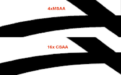
Coverage Sampled AA Example
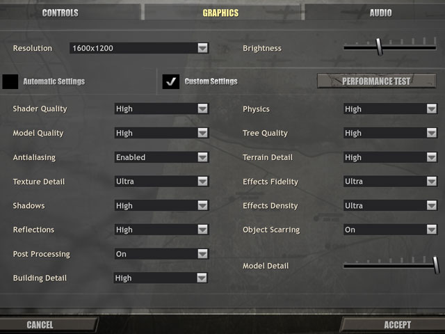
Here I have taken a screen grab from 3DMark06 to show the differences that CSAA can make in image quality. We have 0xAA, 2xAA and 4xAA shown in addition to the 2xAA with 16xCSAA and 4xAA with 16xCSAA screenshots.
To enable CSAA, the game must have AA enabled in the game AND you must set the NVIDIA control panel driver to "enhanced" mode, seen below:


 1600x1200 - 0xAA - CSAA Off - 16xAF - Click to Enlarge
 1600x1200 - 2xAA - CSAA Off - 16xAF - Click to Enlarge
 1600x1200 - 2xAA - CSAA 16x - 16xAF - Click to Enlarge
 1600x1200 - 4xAA - CSAA Off - 16xAF - Click to Enlarge
 1600x1200 - 4xAA - CSAA 16x - 16xAF - Click to Enlarge
In my evaluation of these screen shots, the CSAA mode at 16x setting looks the same whether in the game options are at 2x or 4x; this is the normal behavior. Comparing the image quality of the CSAA enabled screen grabs to the 2xAA setting, there is an obvious improvement. That improvement is less noticeable when compared to the 4xAA image quality, but I'd still have to side with CSAA bringing a slightly better picture to the game.
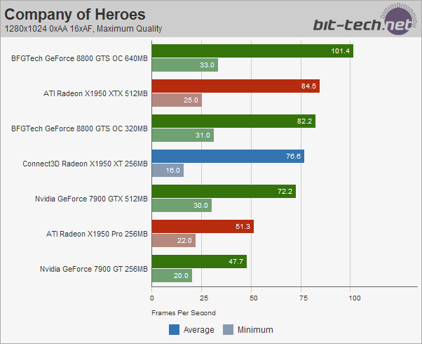
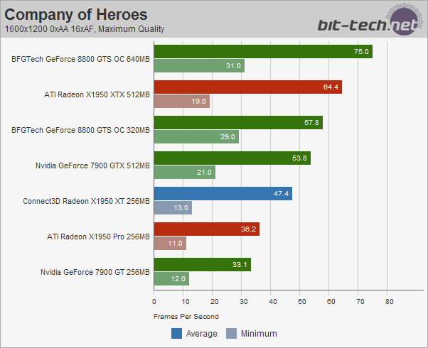
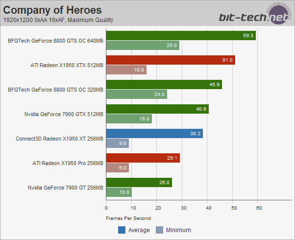
How does this affect performance though?
1600x1200 - 3DMark06 - GT1 |
0xAA |
2xAA |
2xAA16xCSAA |
4xAA |
4xAA16xCSAA |
FPS |
34.017 |
31.022 |
26.257 |
28.023 |
26.251 |
Overall, the performance with CSAA enabled is about on par with standard, in-game 4xAA. And with slightly better image quality to boot, this could make CSAA a well utilized feature in GeForce 8800 cards.
New and Improved Texture Filtering
I mentioned in the discussion on the new G80 architecture that the texture filtering units are much improved and offer us better IQ options than ever before. While we haven't looked at it in depth on PC Perspective recently, there has been a growing concern over the filtering options that both ATI and NVIDIA were setting in their drivers, and the quality they produced. If you have ever been playing a game like Half Life 2 or Guild Wars (probably one of the worst) and noticed "shimmering" along the ground, where textures seem to "sparkle" before they come into focus, then you have seen filtering quality issues.
 ATI X1950 XTX - 16x AF - Default Settings - Click to Enlarge
This first diagram shows us what 16x AF at default settings on the ATI X1950 XTX produces in terms of image quality. In short, anywhere you see the colors banding out wards towards the edge of the screen, filtering will be less in that area. At 45 and 135 degree angles (and their inverses) in the above filtering algorithm, filtering is not done as precisely because of the larger amount of processing required at these angles. This is what produces the shimmering and sparkles you see.
 ATI X1950 XTX - 16x AF - High Quality AF Settings - Click to Enlarge
ATI started offering a new "high quality AF" mode in their Catalyst driver with the X1900 release, and this greatly enhanced the AF quality levels we saw. It also reduced the shimmering effect I had come to despise.
 NV 7900 GTX - 16x AF - Default Settings - Click to Enlarge
On the 7900 GTX, NVIDIA's default settings look much like the ATI default settings did with the same angle issues seen on the ATI cards.
 NV 7900 GTX - 16x AF - High Quality AF Settings - Click to Enlarge
However, even when setting the filtering level to "high quality" NVIDIA's driver does not allow for much improvement in the filtering quality on the 7900.
 NV 8800 GTX - 16x AF - Default Settings - Click to Enlarge
Image quality fanatics rejoice; this is the default setting on the new GeForce 8800 GTX. At 16x AF, the 8800 GTX shows much better filtering quality than even the high quality setting on the ATI X1950 XTX card.
 NV 8800 GTX - 16x AF - High Performance AF Settings - Click to Enlarge
Even when set at "high performance" (which we've never told anyone to do) the 8800 GTX is impressive.
 NV 8800 GTX - 16x AF - High Quality AF Settings - Click to Enlarge
Finally, when setting the 8800 GTX to "high quality" mode in the driver, we see an improvement from the default settings; when you see how much power this card has you might find yourself pretty likely to turn features like this on!
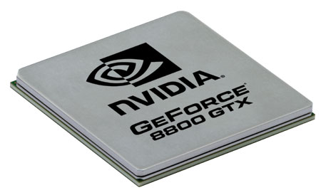
The 8800 GTX and 8800 GTS
NVIDIA's Specifications
After talking about architecture and technology for what seems like forever, let's get down to the actual product you can plug into your system. NVIDIA is releasing two seperate graphics cards today: the GeForce 8800 GTX and the 8800 GTS.
The new flagship is the 8800 GTX card, coming in at an expected MSRP of $599 with a hard launch; you should be able to find these cards for sale today. The clock speed on the card is 575 MHz, but remember that the 128 stream processors run at 1.35 GHz, and they are labeled as the "shader" clock rate here. The GDDR3 memory is clocked at 900 MHz, and you'll be getting 768MB of it, thanks to the memory configuration issue we talked about before. There are dual dual-link DVI ports and an HDTV output as well.

The runner up for today is the 8800 GTS, though it is still a damn fast card. Expected to sell for $449 and should be ready for launch today, the 8800 GTS runs at a core clock speed of 500 MHz and has 96 SPs that run at 1.2 GHz, compared to the 1.35 GHz on the GTX model. The 640MB of GDDR3 memory runs at 800 MHz and the same dual dual-link DVI ports and HDTV output connections are included.
Those of you looking for HDCP support will be glad to know that it is built into the chip, but an external CryptoROM is still necessary (and needs to be included by the board partner) for HDCP to actually function. At first glance, it does look like most of the first run of 8800 GTX cards are going to support HDCP though; GTS cards as well.
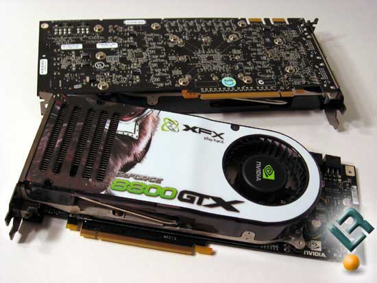
The Reference Sample
The NVIDIA GeForce 8800 GTX card is big; no getting around that. It's about an inch and a half longer than the 7900 GTX cards, though its not really noticeably heavier; the X1950 XTX definitely has it beat there.
 Click to Enlarge
The heatsink on the card is big as well, leaving most of the PCB hidden behind it, save for the far right edge of it. The fan on the dual-slot cooler is pretty quiet, and I didn't have any issues with fan noise like I did with the X1900-series of cards last year.
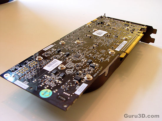
All 768MB of GDDR3 memory is located on the front of the card, and the rear of the PCB is pretty empty.
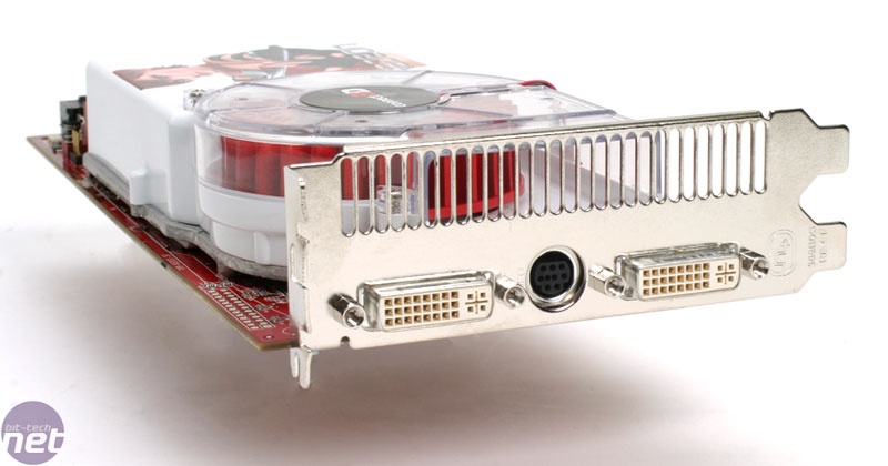
Here you can see the gun-metal color of the case bracket on the card, though I don't know if this is going to be carried over to the retail cards. There are two dual-link DVI connections here, so you can support two of the Dell 30" monitors if you are so included! The TV output port there supports HDTV as well with a dongle that most retailers will include.

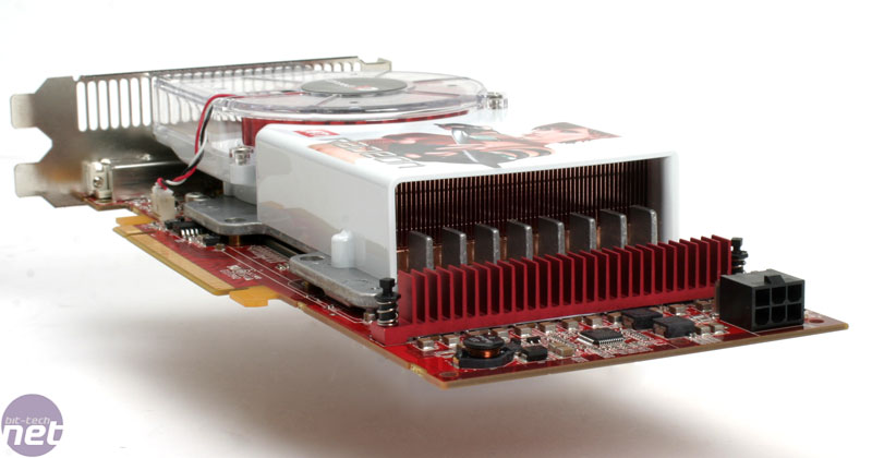
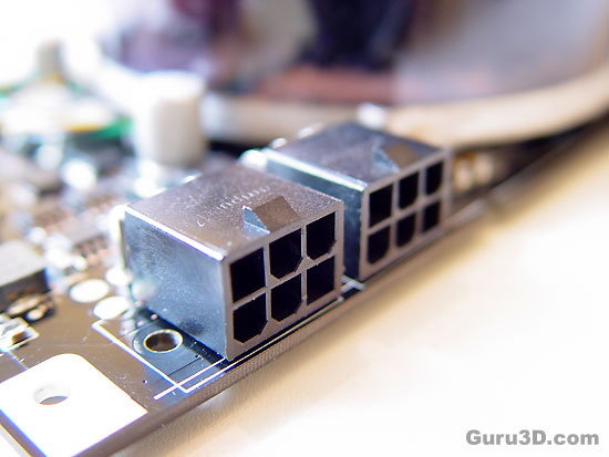
Yeah, you'll notice that there are TWO PCIe power connectors on the GeForce 8800 GTX card (though the 8800 GTS will only require one). NVIDIA says that since the card can pull more than the 150 watts that a single PCIe power connection would technically allow (75 watts from the PCIe port and 75 watts from the single 6-pin connector), they erred on the side of caution by including two. They did allude to another graphics card that pulled more than 150 watts but did NOT have two connections for power...I think that card starts with "X19" and ends with "50 XTX". You are required to connect two power cables though, as leaving one empty will cause the system to beep incessently.

The 8800 GTX is not without an SLI connection, though NVIDIA wasn't ready for SLI at the time of this launch; they are working on final drivers. But, we did notice that there are two SLI connections here,
much like we saw on the ATI X1950 Pro cards last month. This is probably going to be used for chaining more than two cards together in a system.
 Click to Enlarge
Removing the heatsink from the card shows this mammoth chip under the hood...simply...huge. The G80 die is surrounded by a heatsink leveling plate for safety reasons and then by the 12 64MB GDDR3 memory chips.
Using the quarter test, I can officially say the G80 is the biggest chip EVAR!!! Or maybe just the biggest I have tested, but you get the point. How else did you expect 681 million transistors to look? For comparison, below is the ATI X1950 XTX chip next to the SAME quarter.
No camera tricks here!!!
Finally, this little chip off to the side is the NVIDIA TMDS display logic put into a custom ASIC. NVIDIA claims this was done to "simplify package and board routing as well as for manufacturing efficiencies"; sounds like 681 million was the limit to me!


 Likes:


 Responder com Citação


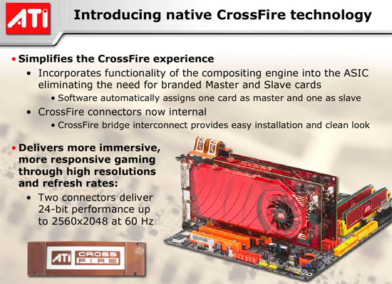
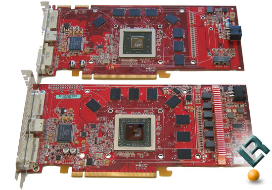
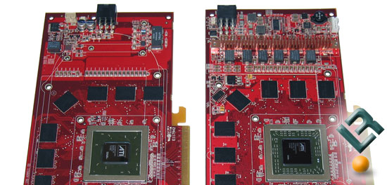
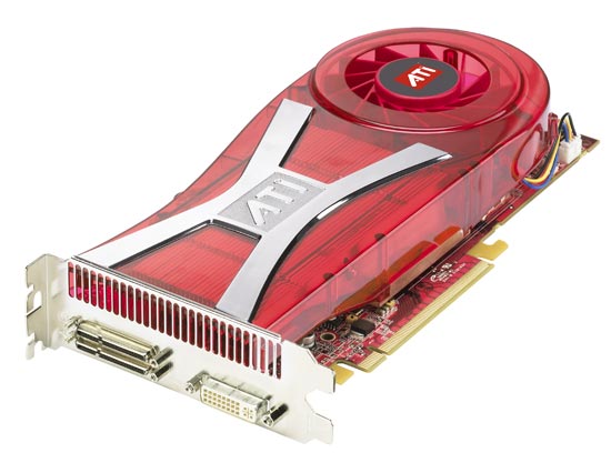
 The RV570 GPU
  A pair of Radeon X1950 Pro cards
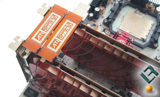
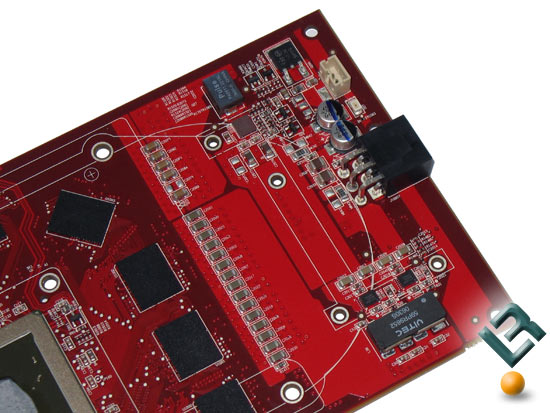
  Each Radeon X1950 Pro has two CrossFire connector, uh, connectors
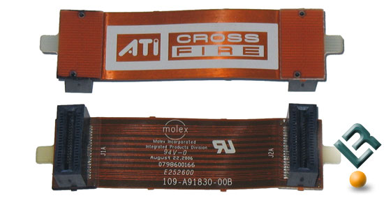
  CrossFire connector (left) and SLI bridge (right)
  Gotta have two links to make it go
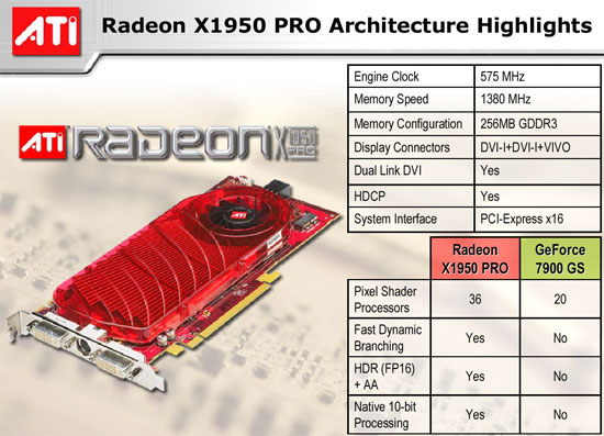
 A new review today as we recently received a fresh product from PowerColor, which coincidentally is launching officially today. It's now October and although slightly delayed ATI gives you the *drum roll* Radeon X1950 Pro!
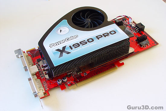


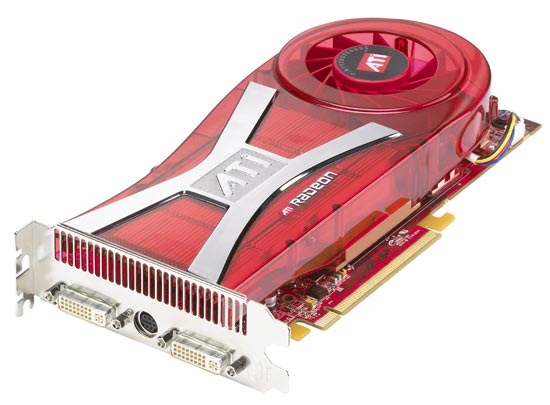
 The Radeon X1950 CrossFire Edition (left) and Radeon X1950 XTX (right)
  The Radeon X1900 XT 256MB (left) and Radeon X1950 XTX (right)
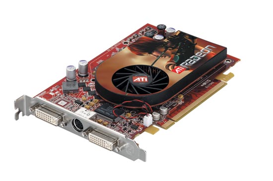
  The Radeon X1650 XT
  Dual dual-link DVI ports flank the X1650 XT's TV-out port


 What you need to understand that the new microarchitecture of the the Dx10 GPU (Graphics Processing Unit) has been changed significantly, the generic elements are all still there.


 So what you need to remember is that CSAA enhances application antialiasing modes with higher quality antialiasing. The new modes are called 8x, 8xQ, 16x, and 16xQ. The 8xQ and 16xQ modes provide first class antialiasing quality TBH.


Bookmarks