

O jogo para a frente tem níveis espetaculares em design, efeitos 3D, isto que vemos aqui é só uma pequena amostra

User Tag List
 Likes: 2
Resultados 16 a 30 de 226
Tópico: História da evolução dos GPU
-
17-01-15, 16:08 #16Tech Ubër-Dominus


- Registo
- Nov 2013
- Local
- City 17
- Posts
- 30,121
- Likes (Dados)
- 0
- Likes (Recebidos)
- 2
- Avaliação
- 1 (100%)
- Mentioned
- 0 Post(s)
- Tagged
- 0 Thread(s)
-
19-01-15, 12:14 #17Moderador

- Registo
- Feb 2013
- Local
- Santo Tirso
- Posts
- 12,672
- Likes (Dados)
- 30
- Likes (Recebidos)
- 208
- Avaliação
- 4 (100%)
- Mentioned
- 7 Post(s)
- Tagged
- 0 Thread(s)
Mais um artigo interessante da Techspot onde 5 gerações de Radeons são comparadas.
Then and Now: 5 Generations of Radeon Graphics Compared
Ryzen R5 3700X / Noctua NH-D15 / B550 AORUS ELITE V2 / Cooler Master H500 Mesh / 16Gb DDR4 @ 3800mhz CL16 / Gigabyte RTX 2070 Super / Seasonic Focus GX 750W / Sabrent Q Rocket 2 TB / Crucial MX300 500Gb + Samsung 250Evo 500Gb / Edifier R1700BT
-
19-01-15, 14:01 #18O Administrador
- Registo
- Mar 2013
- Local
- Multiverso
- Posts
- 17,814
- Likes (Dados)
- 74
- Likes (Recebidos)
- 156
- Avaliação
- 31 (100%)
- Mentioned
- 31 Post(s)
- Tagged
- 0 Thread(s)
Boas! Post Original de Jorge-Vieira

Sim, é verdade lá mais para a frente é fantástico o design 3d para altura... continuo a dizer que o CEU foi algo que mais me fascinou logo á partida... (era animado e dinamico, enquanto que na altura era tudo estático com bitmaps e mais nada)...
Outro jogo dos primordios do 3D foi o P.O.D. e o M.D.K., o primeiro foi lançado na altura que a Intel lançou o pentium MMX com as famosas extensões que davam boost nos processamentos...
Esse vídeo mostra o POD com Glide... Pode parecer datado agora, na altura era cutting EDGE 3D!
Cumprimentos,
LPCMy Specs: .....

CPU: AMD Ryzen 7 5800X3D :-: Board: MSI B550M BAZOOKA :-: RAM: 64 GB DDR4 Kingston Fury Renegade 3600 Mhz CL16 :-: Storage: Kingston NV2 NVMe 2 TB + Kingston NV2 NVMe 1 TB
CPU Cooling Solution: ThermalRight Frost Commander 140 Black + ThermalRight TL-C12B-S 12CM PWM + ThermalRight TL-C14C-S 14CM PWM :-: PSU: Corsair HX 1200 WATTS
Case: NZXT H6 FLOW :-: Internal Cooling: 4x ThermalRight TL-C12B-S 12CM PWM + 4x ThermalRight TL-C14C-S 14CM PWM
GPU: ASUS TUF AMD RADEON RX 7900 XTX - 24 GB :-: Monitor: BenQ EW3270U 4K HDR
-
19-01-15, 14:03 #19O Administrador
- Registo
- Mar 2013
- Local
- Multiverso
- Posts
- 17,814
- Likes (Dados)
- 74
- Likes (Recebidos)
- 156
- Avaliação
- 31 (100%)
- Mentioned
- 31 Post(s)
- Tagged
- 0 Thread(s)
Boas,
Aqui fica um comparativo interessante com todas as placas aceleradoras em 1996 e o POD.
Cumprimentos,
LPCMy Specs: .....
CPU: AMD Ryzen 7 5800X3D :-: Board: MSI B550M BAZOOKA :-: RAM: 64 GB DDR4 Kingston Fury Renegade 3600 Mhz CL16 :-: Storage: Kingston NV2 NVMe 2 TB + Kingston NV2 NVMe 1 TB
CPU Cooling Solution: ThermalRight Frost Commander 140 Black + ThermalRight TL-C12B-S 12CM PWM + ThermalRight TL-C14C-S 14CM PWM :-: PSU: Corsair HX 1200 WATTS
Case: NZXT H6 FLOW :-: Internal Cooling: 4x ThermalRight TL-C12B-S 12CM PWM + 4x ThermalRight TL-C14C-S 14CM PWM
GPU: ASUS TUF AMD RADEON RX 7900 XTX - 24 GB :-: Monitor: BenQ EW3270U 4K HDR
-
19-01-15, 14:08 #20Moderador
- Registo
- Feb 2013
- Local
- Santo Tirso
- Posts
- 12,672
- Likes (Dados)
- 30
- Likes (Recebidos)
- 208
- Avaliação
- 4 (100%)
- Mentioned
- 7 Post(s)
- Tagged
- 0 Thread(s)
Excelente partilha Post Original de Lord Paulus Cobris
 Ryzen R5 3700X / Noctua NH-D15 / B550 AORUS ELITE V2 / Cooler Master H500 Mesh / 16Gb DDR4 @ 3800mhz CL16 / Gigabyte RTX 2070 Super / Seasonic Focus GX 750W / Sabrent Q Rocket 2 TB / Crucial MX300 500Gb + Samsung 250Evo 500Gb / Edifier R1700BT
-
19-01-15, 15:06 #21Tech Ubër-Dominus
- Registo
- Nov 2013
- Local
- City 17
- Posts
- 30,121
- Likes (Dados)
- 0
- Likes (Recebidos)
- 2
- Avaliação
- 1 (100%)
- Mentioned
- 0 Post(s)
- Tagged
- 0 Thread(s)
Muito boa partilha, esse video mostra muito bem o quanto as 3DFX eram dominantes nos graficos 3D.
-
02-02-15, 16:57 #22Moderador
- Registo
- Feb 2013
- Local
- Santo Tirso
- Posts
- 12,672
- Likes (Dados)
- 30
- Likes (Recebidos)
- 208
- Avaliação
- 4 (100%)
- Mentioned
- 7 Post(s)
- Tagged
- 0 Thread(s)
Fica aqui um artigo interessante sobre como funcionam os cooler modernos de vários fabricantes de GPUs.
GPU Cooler Differences: Defining ACX, Frozr, Vapor X, WindForce, & DirectCU
Para quem quiser aprender mais um pouco, também temos este artigo do mesmo site, a falar de como funcionam os coolers actuais para CPUs.
Understanding CPU Heatsinks: Picking the Best CPU Cooler
Ryzen R5 3700X / Noctua NH-D15 / B550 AORUS ELITE V2 / Cooler Master H500 Mesh / 16Gb DDR4 @ 3800mhz CL16 / Gigabyte RTX 2070 Super / Seasonic Focus GX 750W / Sabrent Q Rocket 2 TB / Crucial MX300 500Gb + Samsung 250Evo 500Gb / Edifier R1700BT
-
24-04-15, 17:16 #23Tech Ubër-Dominus
- Registo
- Nov 2013
- Local
- City 17
- Posts
- 30,121
- Likes (Dados)
- 0
- Likes (Recebidos)
- 2
- Avaliação
- 1 (100%)
- Mentioned
- 0 Post(s)
- Tagged
- 0 Thread(s)
AMD's Graphics Core Next Preview: AMD's New GPU, Architected For Compute
Toda a noticia:We’ve just returned from sunny Bellevue, Washington, where AMD held their first Fusion Developer Summit (AFDS). As with other technical conferences of this nature such as NVIDIA’s GTC and Intel’s IDF, AFDS is a chance for AMD to reach out to developers to prepare them for future products and to receive feedback in turn. While AMD can make powerful hardware it’s ultimately the software that runs on it that drives sales, so it’s important for them to reach out to developers to ensure that such software is being made.
AFDS 2011 served as a focal point for several different things going on at AMD. At its broadest, it was a launch event for Llano, AMD’s first mainstream Fusion APU that launched at the start of the week. AMD has invested the future of the company into APUs, and not just for graphical purposes but for compute purposes too. So Llano is a big deal for the company even though it’s only a taste of what’s to come.
The second purpose of course was to provide sessions for developers to learn more about how to utilize AMD’s GPUs for compute and graphics tasks. Microsoft, Acceleware, Adobe, academic researchers, and others were on hand to provide talks on how they’re using GPUs in current and future projects.
The final purpose – and what is going to be most interesting to most outside observers – was to prepare developers for what’s coming down the pipe. AMD has big plans for the future and it’s important to get developers involved as soon as is reasonably possible so that they’re ready to use AMD’s future technologies when they launch. Over the next few days we’ll talk about a couple of different things AMD is working on, and today we’ll start with the first and most exciting project: AMD Graphics Core Next.
Graphics Core Next (GCN) is the architectural basis for AMD’s future GPUs, both for discrete products and for GPUs integrated with CPUs as part of AMD’s APU products. AMD will be instituting a major overhaul of its traditional GPU architecture for future generation products in order to meet the direction of the market and where they want to go with their GPUs in the future.
While graphics performance and features have been and will continue to be important aspects of a GPU’s design, AMD and the rest of the market have been moving towards further exploiting the compute capabilities of GPUs, which in the right circumstances are capable of being utilized as massive parallel processors that can complete a number of tasks in the fraction of the time as a highly generalized CPU. Since the introduction of shader-capable GPUs in 2002, GPUs have slowly evolved to become more generalized so that their resources can be used for more than just graphics. AMD’s most recent shift was with their VLIW4 architecture with Cayman late last year; now they’re looking to make their biggest leap yet with GCN.
GCN at its core is the basis of a GPU that performs well at both graphical and computing tasks. AMD has stretched their traditional VLIW architecture as far as they reasonably can for computing purposes, and as more developers get on board for GPU computing a clean break is needed in order to build a better performing GPU to meet their needs. This is in essence AMD’s Fermi: a new architecture and a radical overhaul to make a GPU that is as monstrous at computing as it is at graphics. And this is the story of the architecture that AMD will be building to make it happen.
Finally, it should be noted that the theme of AFDS 2011 was heterogeneous computing, as it has become AMD’s focus to get developers to develop heterogeneous applications that effectively utilize both AMD’s CPUs and AMD’s GPUs. Ostensibly AFDS is a conference about GPU computing, but AMD’s true strength is not their CPU side or their GPU side, it’s the combination of the two. Bulldozer will be the first half of AMD’s future APUs, while GCN will be the other half.
http://www.anandtech.com/show/4455/a...ts-for-compute
Um artigo interessante que explica a arquitetura GCN da AMD
-
24-04-15, 17:17 #24Tech Ubër-Dominus
- Registo
- Nov 2013
- Local
- City 17
- Posts
- 30,121
- Likes (Dados)
- 0
- Likes (Recebidos)
- 2
- Avaliação
- 1 (100%)
- Mentioned
- 0 Post(s)
- Tagged
- 0 Thread(s)
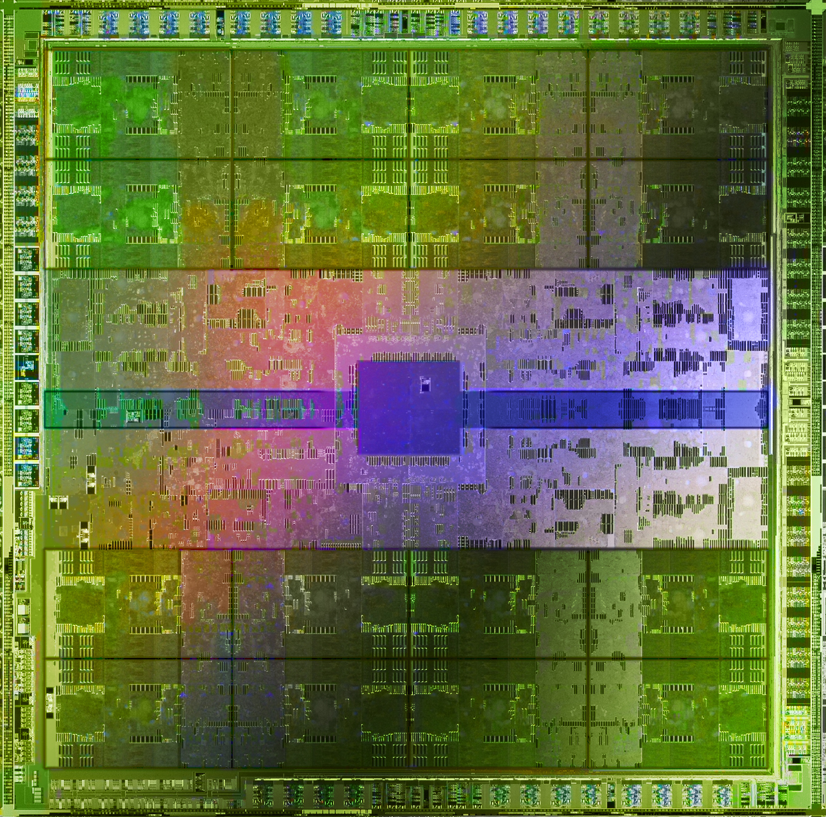
NVIDIA’s GF100: Architected for Gaming
Toda a noticia:At this year’s Consumer Electronics Show, NVIDIA had several things going on. In a public press conference they announced 3D Vision Surround and Tegra 2, while on the showfloor they had products o’plenty, including a GF100 setup showcasing 3D Vision Surround.
But if you’re here, then what you’re most interested in is what wasn’t talked about in public, and that was GF100. With the Fermi-based GF100 GPU finally in full production, NVIDIA was ready to talk to the press about the rest of GF100, and at the tail-end of CES we got our first look at GF100’s gaming abilities, along with a hands-on look at some unknown GF100 products in action. The message NVIDIA was trying to send: GF100 is going to be here soon, and it’s going to be fast.
Before we get too far ahead of ourselves though, let’s talk about what we know and what we don’t know.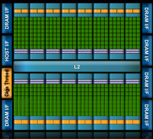
Fermi/GF100 as announced in September of 2009
During CES, NVIDIA held deep dive sessions for the hardware press. At these deep dives, NVIDIA focused on 3 things: Discussing GF100’s architecture as is relevant for a gaming/consumer GPU, discussing their developer relations program (including the infamous Batman: Arkham Asylum anti-aliasing situation), and finally demonstrating GF100 in action on some games and some productivity applications.
Many of you have likely already seen the demos, as videos of what we saw have already been on YouTube for a few days now. What you haven’t seen and what we’ll be focusing on today, is what we’ve learned about GF100 as a gaming GPU. We now know everything about what makes GF100 tick, and we’re going to share it all with you.
With that said, while NVIDIA is showing off GF100, they aren’t showing off the final products. As such we can talk about the GPU, but we don’t know anything about the final cards. All of that will be announced at a later time – and no, we don’t know that either. In short, here’s what we still don’t know and will not be able to cover today: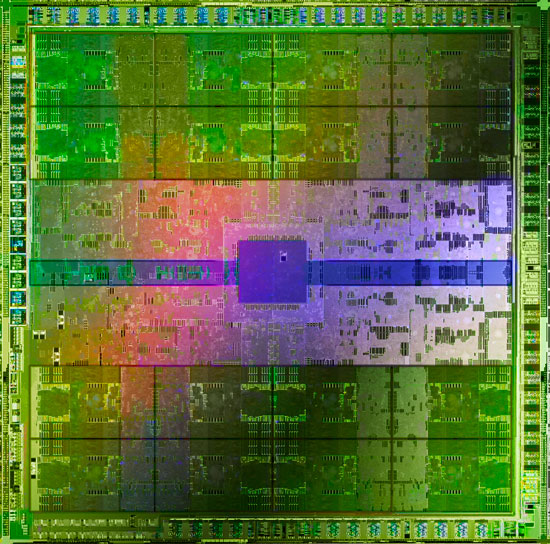
- Die size
- What cards will be made from the GF100
- Clock speeds
- Power usage (we only know that it’s more than GT200)
- Pricing
- Performance
At this point the final products and pricing are going to heavily depend on what the final GF100 chips are like. The clockspeeds NVIDIA can get away with will determine power usage and performance, and by extension of that, pricing. Make no mistake though, NVIDIA is clearly aiming to be faster than AMD’s Radeon HD 5870, so form your expectations accordingly.
For performance in particular, we have seen one benchmark: Far Cry 2, running the Ranch Small demo, with NVIDIA running it on both their unnamed GF100 card and a GTX285. The GF100 card was faster (84fps vs. 50fps), but as Ranch Small is a semi-randomized benchmark (certain objects are in some runs and not others) and we’ve seen Far Cry 2 to be CPU-limited in other situations, we don’t put much faith in this specific benchmark. When it comes to performance, we’re content to wait until we can test GF100 cards ourselves.
With that out of the way, let’s get started on GF100.
http://www.anandtech.com/show/2918
Um artigo que explica em detalhe a arquitetura Fermi da nvidia.
-
27-04-15, 14:39 #25Tech Ubër-Dominus
- Registo
- Nov 2013
- Local
- City 17
- Posts
- 30,121
- Likes (Dados)
- 0
- Likes (Recebidos)
- 2
- Avaliação
- 1 (100%)
- Mentioned
- 0 Post(s)
- Tagged
- 0 Thread(s)
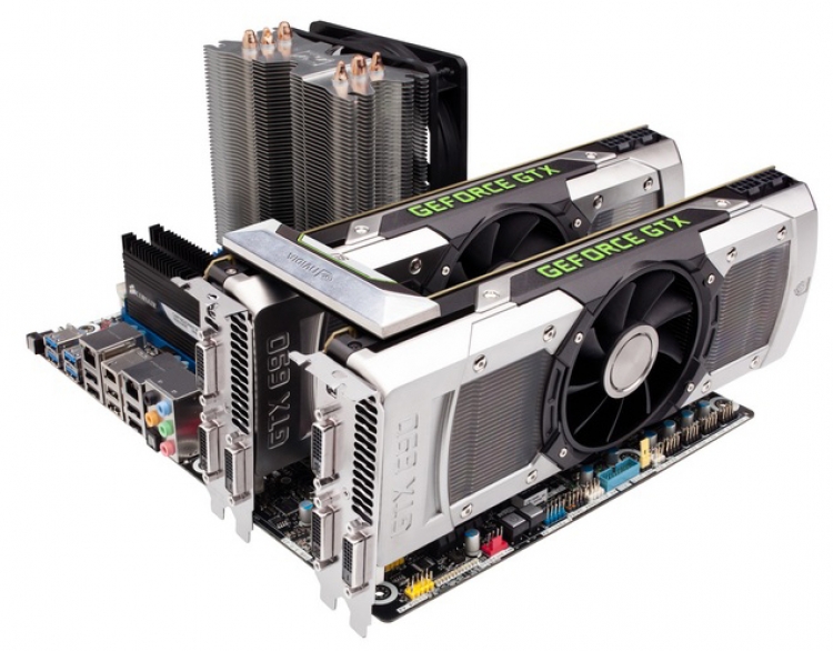
Nvidia's SLI Technology In 2015: What You Need To Know
Todo o artigo:I've been excited by SLI ever since it was introduced as Scan Line Interleave by 3Dfx. Two Voodoo2 cards could operate together, with the noticeable benefit of upping your maximum 3D resolution from 800x600 to 1024x768. Amazing stuff...back in 1998.

Fast forward almost twenty years. 3Dfx went out of business long ago (it was acquired in 2000 out of bankruptcy by Nvidia), and SLI was re-introduced and re-branded by Nvidia in 2004 (it now stands for Scalable Link Interface). But the overall perception of SLI as a status symbol in hardcore gaming machines, offering massive rendering power, but also affected by numerous technical issues, has changed little.
Today we're looking at the green team specifically, and we plan to follow up with a second part on AMD's CrossFire. In that next piece, you'll see us compare both manufactures' dual-GPU offerings.
In this article, we'll explore some of the technology's basics as it operates today, take an in-depth look at scaling with two cards compared to one, discuss driver and game-related issues, explore overclocking potential and finally provide some recommendations on how to decide whether SLI is right for you.
While SLI technically supports up to four GPUs in certain configurations, it is generally accepted that three- and four-way SLI don't scale as well as a two-way array. While you are likely to see PCs with three or four GPUs at the top of synthetic benchmark charts, they're a lot less common in the real world, and not just because of their cost.
Furthermore, Nvidia representatives confirm that three-way SLI is not supported in 8x/4x/4x PCIe lane configurations, which are native to Intel's LGA 1150 platform. You'll either need an LGA 1150-based board equipped with an (expensive) PLX bridge chip or an even more expensive LGA 2011-v3 platform if you want to go beyond two-way SLI. Fortunately, most Haswell/Ivy Bridge/Sandy Bridge platforms enable two-way SLI without issue.
Finally, another downside of going beyond two-way SLI is that, because of the way SLI works, input lag increases as the number of cards working together goes up.
MORE: Best Graphics Cards For The Money
MORE: How To Build A PC: From Component Selection To Installation
MORE: Gaming At 3840x2160: Is Your PC Ready For A 4K Display
MORE: All Graphics Articles
MORE: Graphics Cards in the Forum
What You Need For An SLI Build
In order to build a SLI-capable system, you need the following:
- A motherboard with at least two free PCIe x16 slots, operating in at least in x8 mode (Nvidia does not support SLI on x4 links). Pretty much all LGA 2011, LGA 2011-v3 and LGA 1150 motherboards satisfy this requirement.
- Two (or more) identical Nvidia-based cards that support SLI, or a dual-GPU card like the GeForce GTX 690 or Titan Z. Generally, different cards won't do the trick.
- A suitable power supply. Increasing the number of GPUs in a system rapidly increases its power requirements. Take that into account when you choose your PSU.
- An SLI bridge. This is generally provided by your motherboard's manufacturer as a bundled accessory.
- The latest Nvidia drivers. If you're reading this article, we're pretty sure that you know that you can grab these from Nvidia's website.
In addition, you'll want a relatively enthusiast-oriented CPU, especially if you're shooting for high frame rates (such as to power 120+ Hz displays) more than better eye candy. For reference, the Core i7-4770K overclocked to 4.4 GHz that we used in these tests appeared to cap out at roughly 150 FPS at 1440p in most applications.
Once all of this is sorted out, you can go ahead and enable SLI in the Nvidia Control Panel.
How SLI Works
There are five SLI rendering modes available: Alternate Frame Rendering (AFR), Split Frame Rendering (SFR), Boost Performance Hybrid SLI, SLIAA and Compatibility mode. In practice, however, you can forget about the latter four. Modern games almost exclusively use AFR.
AFR, in Nvidia's own definition, is:
[In AFR mode] "the driver divides workload by alternating GPUs every frame. For example, on a system with two SLI enabled GPUs, frame 1 would be rendered by GPU 1, frame 2 would be rendered by GPU 2, frame 3 would be rendered by GPU 1, and so on. This is typically the preferred SLI rendering mode as it divides workload evenly between GPUs and requires little inter-GPU communication."
 In the most-common SLI AFR rendering mode, GPUs take turns at rendering frames
In order to benefit from performance scaling, individual applications need a so-called SLI profile that tells the display driver what specific form of synchronization is required, and which others can be skipped. Nvidia creates these profiles and releases them as part of its periodic driver upgrades. Newer games may not have SLI profiles available when they launch, or the SLI profile initially released may be buggy (creating visual artifacts) or not yet optimized (limiting scaling).
For more information, please refer to this white paper published on Nvidia's developer network. We encourage all of you who wish to learn more about the technology to read it: SLI_Best_Practices_2011_Feb.
http://www.tomshardware.com/reviews/...-faq,4079.html
-
27-04-15, 14:53 #26O Administrador
- Registo
- Mar 2013
- Local
- Multiverso
- Posts
- 17,814
- Likes (Dados)
- 74
- Likes (Recebidos)
- 156
- Avaliação
- 31 (100%)
- Mentioned
- 31 Post(s)
- Tagged
- 0 Thread(s)
Boas!
SLI E CF vão operar de forma diferente no futuro com o DX12 e o Vulkan.
Vão ser considerados GPU´s agnosticos no API e poderão processar alternadamente independentemente da marca e modelo.
É feito um processamento através do balanceamento da carga vs frames pedidos...
Ou seja é possível misturar marcas e arquitecturas diferentes e até memórias diferentes para o API Pool.
O que irá acontecer é que se um gpu for 75% mais poderoso que o segundo GPU, o primeiro irá processar 75% dos frames e o segundo apenas 25% dos frames.
Isso depois será gerido em low level antes da composição final do frame.
Portanto á partida todos os gpus incluindo os IGP´s podem processar em conjunto com os GPU´s normais e se obter algum benefício no processo.
A memória deixa também de ser duplicada para o framebuffer e passa a ser apenas usada 1x e distribuida pela API Pool...
Portanto um GPU com 4GB e outro com 2GB irá dar 6GB de framebuffer combinado.
Cumprimentos,
LPCMy Specs: .....
CPU: AMD Ryzen 7 5800X3D :-: Board: MSI B550M BAZOOKA :-: RAM: 64 GB DDR4 Kingston Fury Renegade 3600 Mhz CL16 :-: Storage: Kingston NV2 NVMe 2 TB + Kingston NV2 NVMe 1 TB
CPU Cooling Solution: ThermalRight Frost Commander 140 Black + ThermalRight TL-C12B-S 12CM PWM + ThermalRight TL-C14C-S 14CM PWM :-: PSU: Corsair HX 1200 WATTS
Case: NZXT H6 FLOW :-: Internal Cooling: 4x ThermalRight TL-C12B-S 12CM PWM + 4x ThermalRight TL-C14C-S 14CM PWM
GPU: ASUS TUF AMD RADEON RX 7900 XTX - 24 GB :-: Monitor: BenQ EW3270U 4K HDR
-
08-06-15, 14:43 #27Tech Ubër-Dominus
- Registo
- Nov 2013
- Local
- City 17
- Posts
- 30,121
- Likes (Dados)
- 0
- Likes (Recebidos)
- 2
- Avaliação
- 1 (100%)
- Mentioned
- 0 Post(s)
- Tagged
- 0 Thread(s)
ASUS Auto-Extreme Technology – Fully Automated Video Card Production
Noticia:image: http://www.legitreviews.com/wp-conte...gy-645x367.jpg
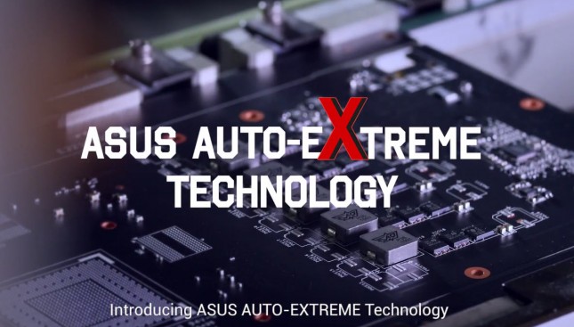
ASUS graphics cards are now produced with ASUS Auto-Extreme technology. This is a new 100% automated manufacturing process, which is an industry-first 100% according to ASUS. Until today all graphics cards being produced required people to hand place the larger components on the circuit board or PCB as many call it. ASUS has achieved 100% automation and is still able to use aerospace-grade Super Alloy Power II components for unsurpassed quality and reliability. It took years of work and over 180 innovations to make this idea a reality. The technology is said to improve the quality of the graphics card and allowing for greating overclocking stability of the boards components. This is because no flux is needed with this new process and ASUS is able to skip a an entire stage of heating in the product process. No flux also means less dust buildup and oxidation on the circuit board and connectors. This process also helps ASUS save money as it reduces the number of employees they need to hire for the assembly line, reduces the use of harsh chemicals and they are able to reduce electricity consumption by 50%!
ASUS Auto-Extreme Technology also allows ASUS to create circuit boards that are completely smooth as everything is surface mounted for the very first time thanks to Surface Mounted Technology (SMT). This means no more pins and prongs will be poking you on the back of the board when you are installing your video card in your gaming PC since board components are soldered onto pads on the board itself rather than placed through holes on the PCB. ASUS believes this moves them a step closer to producing the best graphics card possible.
You can see ASUS Auto-Extreme Technology in action on the video below. The video also features ASUS Chief Engineer of Graphcis Cards Mr. Ken Liu himself!
http://www.legitreviews.com/asus-aut...MuiVlgPaC0F.99
-
27-06-15, 21:48 #28Tech Ubër-Dominus
- Registo
- Nov 2013
- Local
- City 17
- Posts
- 30,121
- Likes (Dados)
- 0
- Likes (Recebidos)
- 2
- Avaliação
- 1 (100%)
- Mentioned
- 0 Post(s)
- Tagged
- 0 Thread(s)
The IP licensing business model. A love story.
Toda a noticia:Business Model Based on Partnerships
Some months ago my colleague Rys Sommefeldt wrote an article offering his (deeply) technical perspective on how a chip gets made, from R&D to manufacturing. While his bildungsroman production covers a lot of the engineering details behind silicon production, it is light on the business side of things; and that is a good thing because it gives me opportunity to steal some of his spotlight!
Alexandru Voica works for Imagination Technologies. His background includes research in computer graphics at the School of Advanced Studies Sant'Anna in Pisa and a brief stint as a CPU engineer, working on several high-profile 32-bit processors used in many mobile and embedded devices today. You can follow Alex on Twitter @alexvoica.
This article will give you a breakdown of the IP licensing model, describing the major players and the relationships between them. It is not designed to be a complete guide by any means and some parts might already sound familiar, but I hope it is a comprehensive overview that can be used by anyone who is new to product manufacturing in general.
The diagram below offers an analysis of the main categories of companies involved in the semiconductor food chain. Although I’m going to attempt to paint a broad picture, I will mainly offer examples based on the ecosystem formed around Imagination (since that is what I know best).

A simplified view of the manufacturing chain
Let’s work our way from left to right.
IP vendors
Traditionally, these are the companies that design and sell silicon IP. ARM and Imagination Technologies are perhaps the most renowned for their sub-brands: Cortex CPU + Mali GPU and MIPS CPU + PowerVR GPU, respectively.
Given the rapid evolution of the semiconductor market, such companies continue to evolve their business models beyond point solutions to become one-stop shops that offer more than for a wide variety of IP cores and platforms, comprising CPUs, graphics, video, connectivity, cloud software and more.
Continue reading The IP licensing business model. A love story. on PC Perspective!!
For example, Imagination has recently announced an entire range of reference IP platforms designed to accommodate the rapidly shifting IoT market. Take the smart sensor IP platform below: not only does it include the full hardware IP required to build a chip (a MIPS Warrior MCU and an Ensigma Whisper RPU), but it also comes pre-bundled with all the additional software required to connect the device to the cloud (the FlowCloud IoT API). Moving up the performance ladder, we find the connected audio IP platform, built around Caskeid – an innovative combination of hardware and software IP that delivers pitch-perfect wireless audio streaming.

IP platforms using MIPS, PowerVR and Ensigma
Revenue model
For any new deal signed, the IP vendor will charge an up-front premium called a license fee.
Based on factors such as the complexity of the IP, cost of development, target applications and expected volumes, a license fee can vary from 100,000s to 1,000,000s of dollars.
Once products using the IP start shipping, the vendor will also receive royalties. They represent a fraction of the total chip cost and can be between a few cents to tens of cents, depending on a range of factors, including the ASP (Average Selling Price) of a processor.
The royalty rate also varies over time as companies move to larger volumes.

Revenue vs. investment curves for IP
The diagram above shows you how the ideal relationship between investment and revenue for IP; notice how companies must make a significant financial investment if they want to see a jump in revenue once that piece of IP reaches maturity.
The revenue curve assumes that mature IP eventually ships in extremely high volume, generating a significant return on the initial investment.
Deliverables
In terms of deliverables, there are generally two types of licensable hardware IP:
- Off-the-shelf processor IP: fully designed and pre-verified RTL code (e.g. a PowerVR G6230 GPU) configured according to a customer’s specifications. This sounds like a trivial process but actually can turn out to be a very complex task; for example, you can read this article that describes how Imagination helps customers pick a PowerVR GPU for a 4K DTV and a smartwatch.
- Architectural license: the semiconductor vendor receives the rights to design their own hardware implementation based on a set of specifications. Typically, an architectural license is granted when a silicon company with a significant internal design capability wants to radically differentiate from the competition or when it wants to target a specific market that is not served by existing, pre-designed off-the-shelf processor IP (or sometimes both). Some IP companies simply hand over the handbook and an architectural validation suite for a hefty fee and wash their hands clean; others take a different approach, working with the architectural licensee to offer a skeleton on which the SoC designer can build on (if needed).
Read When SoC met IP to learn more about the implications of licensing off-the-shelf IP and/or an entire hardware architecture.
Any license has complex legal implications but generally an SoC company looking to purchase IP will be presented with three options:
- Single use: the silicon vendor is licensing one IP block (e.g. a MIPS P5600 CPU) for use in one chip
- Multiple use: the silicon vendor is licensing one IP block (e.g. a PowerVR G6200 GPU) for use in multiple chips (e.g. a mobile SoC and a TV chip)
- Subscription: the silicon vendor has unlimited access to an entire family/generation of IP (e.g. PowerVR Series6) and can use it in multiple chips
In addition, many IP vendors develop in-house physical IP to help SoC designers hit specific targets. Take the Design Optimization Kits (DOKs) for entry-level PowerVR Rogue GPUs for example: it is essentially a pre-verified package guaranteed to fit in a certain silicon area – a vital requirement for that specific market; there are also DOKs optimized to hit the high performance efficiency goals of the premium market.

Imagination + Synopsys DOK
DOKs are usually created for two processors in a family: the most popular (e.g. PowerVR G6200) and the smallest (e.g. PowerVR G6100).
The combination of the two guarantees you will likely hit the maximum number of customers interested in licensing from any given generation of IP.
Fabless semiconductor vendors
Fabless semiconductor companies like Actions Semiconductor, Allwinner Technology, AMD, Broadcom, Marvell, MediaTek, Microchip, Qualcomm, Rambus, Rockchip, Realtek, Xilinx – and the list goes on – are designers of the semiconductors that power many of our electronic products.
There are two main routes for fabless chip makers to design (parts of) an SoC: license from an IP vendor or produce your own in-house design. According to a recent chart presented at the 2015 Imagination Summit in Santa Clara, designing in-house processors takes 3-4 years and costs between 100-200 million dollars, on average. Meanwhile, licensing IP cuts the cost to $10-$50 million and reduces design time in half.
Another remarkable phenomenon is the degree of consolidation occurring in the semiconductor space; in the last three years alone, there have been some huge mergers and acquisitions – NXP/Freescale, Avago/Broadcom, and Intel/Altera being the most recent examples.

NVIDIA Tegra X1
One aspect that usually goes unnoticed is the amount of effort that goes into marketing a chip. Gone are the days when all you had to do is take a design into mass production and then simply count on the OEM to do the rest of the heavy lifting for you; now semiconductor vendors have to produce full reference platforms (notice a trend here?). Some even become a full-fledged OEM and start selling directly to consumers.
This occurs especially in regions like Asia where OEMs rely heavily on chip makers to ‘hunker down and git’er done’ – and sometimes that even means building a fully-certified, ready to ship device. Through collaboration with OEM/ODMs some semiconductor manufacturers are changing their value proposition and helping to deliver more complete devices to consumers.

Intel smartphone reference design
Finally, the consumer gets a device that costs considerably less than a similarly-specced flagship product.
http://www.pcper.com/reviews/Mobile/...del-love-story
-
03-07-15, 14:18 #29Tech Ubër-Dominus
- Registo
- Nov 2013
- Local
- City 17
- Posts
- 30,121
- Likes (Dados)
- 0
- Likes (Recebidos)
- 2
- Avaliação
- 1 (100%)
- Mentioned
- 0 Post(s)
- Tagged
- 0 Thread(s)
Crossfire and SLI market is just 300.000 units
Tendo em conta o mercado de PC, pensei que este número fosse bem superior.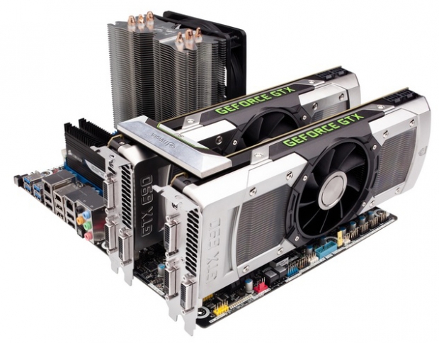
Insider confirms
Next time you get to complain about the lack of SLI support or Crossfire support, you will have to remember this number.
According to our well informed industry insiders, there are only about 300,000 people who own SLI or Crossfire setups. This doesn’t sound like a big number at all, considering that the PC gaming market, according to Jon Peddie Research, is a $21.7 billion market. This number combines CPUs, motherboards, GPUs, Monitors, peripherals, SSD and everything else you need to play games on a PC.
It is hard to find the right numbers on how many GPUs Nvidia or AMD sell, but you would expect that SLI and Crossfire enthusiasts capture a bit more than 0.3 million. This can also give you an idea that the GPUs we can so much about, including Geforce GTX Titan, Geforce GTX 980 TI or AMD Radeon Fury X are a tiny fraction of overall sales.
What we have been preaching for a while these 300K people really know what they are doing, most of them at least. These are usually super high end enthusiasts, spending a lot of time on forums, comment sections of tech websites. They are very opinionated and they are really passionate about who they support - AMD or Nvidia.
In case you are one of these 300,000 you should feel special, as not too many people spend $1,000 to $2,000 on two GPUs. In case the game supports it, and in case that the driver is there, there is no doubt that two cards are better than one. The big obstacle is that two cards e.g. Fury X usually cost twice as much as one Fury X card. The same logic applies to GTX 980 TI cards, and let's not forget that you also need a better PSU, chassis and so on.
Jon Peddie researchers are quite certain that the gaming market will grow from the existing $21.71 billion to $23.11 billion market by 2017, and with that we expect that the number of SLI and Crossfire setups will grow.
Innovations like G-Sync and FreeSync have definitely boosted monitor sales and many people want to get 3840x2160 aka 4K monitors or some curved or wide screen monitors to make their gaming better.
In case you own a mainstream card such as the Geforce GTX 760 / 960 or Radeon R9 280 / 380, don’t be sad, you are still better off than more than 50 percent of market that are stuck with Intel integrated graphics. According to a Steam survey, the most popular "graphics card" in the world is still Intel HD Graphics 4000.
-
03-07-15, 16:48 #30O Administrador
- Registo
- Mar 2013
- Local
- Multiverso
- Posts
- 17,814
- Likes (Dados)
- 74
- Likes (Recebidos)
- 156
- Avaliação
- 31 (100%)
- Mentioned
- 31 Post(s)
- Tagged
- 0 Thread(s)
Boas!
Grande supresa!
Pensei também que fossem bem mais pessoas a usar o sli e CF...
Isto só mostra como existe ainda muito medo e desconhecimento de meter mais que uma gráfica...
As histórias de terror do passado ainda assombram estas tecnologias...
Será que isso mudará com o DX12?
O tempo o dirá...
Cumprimentos,
LPCMy Specs: .....
CPU: AMD Ryzen 7 5800X3D :-: Board: MSI B550M BAZOOKA :-: RAM: 64 GB DDR4 Kingston Fury Renegade 3600 Mhz CL16 :-: Storage: Kingston NV2 NVMe 2 TB + Kingston NV2 NVMe 1 TB
CPU Cooling Solution: ThermalRight Frost Commander 140 Black + ThermalRight TL-C12B-S 12CM PWM + ThermalRight TL-C14C-S 14CM PWM :-: PSU: Corsair HX 1200 WATTS
Case: NZXT H6 FLOW :-: Internal Cooling: 4x ThermalRight TL-C12B-S 12CM PWM + 4x ThermalRight TL-C14C-S 14CM PWM
GPU: ASUS TUF AMD RADEON RX 7900 XTX - 24 GB :-: Monitor: BenQ EW3270U 4K HDR


 Responder com Citação

Informação da Thread
Users Browsing this Thread
Estão neste momento 2 users a ver esta thread. (0 membros e 2 visitantes)
 Regras
São agora 04:36.
 User Alert System provided by
Advanced User Tagging v3.3.0 (Lite) -
vBulletin Mods & Addons Copyright © 2024 DragonByte Technologies Ltd.
User Alert System provided by
Advanced User Tagging v3.3.0 (Lite) -
vBulletin Mods & Addons Copyright © 2024 DragonByte Technologies Ltd.
Feedback Buttons provided by Advanced Post Thanks / Like (Lite) - vBulletin Mods & Addons Copyright © 2024 DragonByte Technologies Ltd.
Portugal-Tech 2012-24 | Todos os direitos reservados! Alojamento Powered by: Trignosfera
Powered by vBulletin® Version 4.2.5 Alpha 3
Copyright © 2024 vBulletin Solutions, Inc. All rights reserved.
Copyright © 2024 vBulletin Solutions, Inc. All rights reserved.
Feedback Buttons provided by Advanced Post Thanks / Like (Lite) - vBulletin Mods & Addons Copyright © 2024 DragonByte Technologies Ltd.
Portugal-Tech 2012-24 | Todos os direitos reservados! Alojamento Powered by: Trignosfera
Bookmarks