

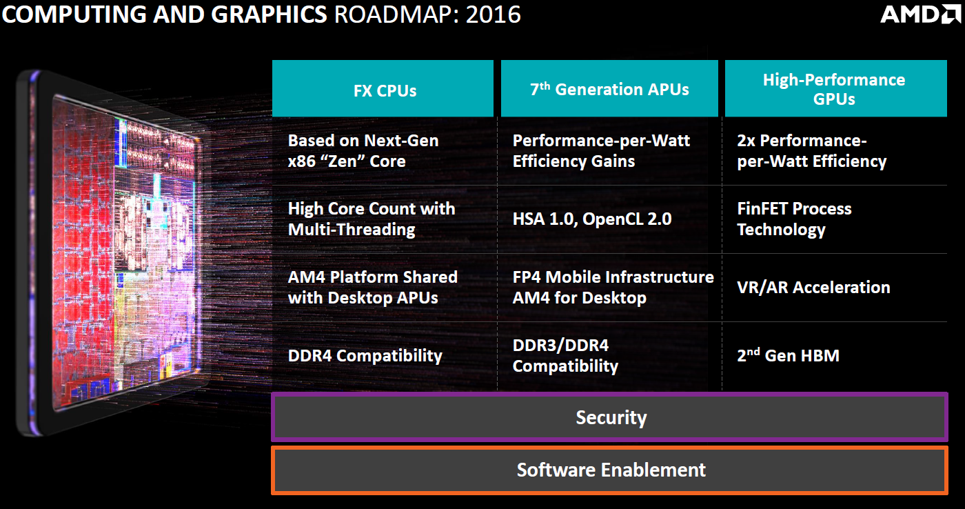
AMD: We have very strong roadmap for GCN architecture
Noticia:Despite of ongoing problems and lowering research and development budget, Advanced Micro Devices maintains optimism and claims that it will keep financing development of key products.
In the recent months, Advanced Micro Devices has been criticized heavily for re-introducing its previous-generation graphics processing units under new names. The release of one new GPU per year is clearly a result of multiple business decisions, massive layoffs from the company several years ago as well as limited research and development budget. Nonetheless, AMD seems to remain rather optimistic and claims that it has strong APU, CPU and GPU roadmaps. What is particularly interesting is that the company intends to continue improving its GCN [graphics core next] architecture, not introduce something brand new.
Where weve been incredibly protective in maintained investment is in where we are banking the future of the company, said Mark Papermaster, chief technology officer of AMD, at the at Pacific Crest annual global technology leadership forum, reports Tech Trader Daily. So it is on that next generation of CPUs starting with Zen. It is on successive generations of our graphics core next. Huge volume in what we have in not only in discrete graphics and our APU, but the game console wins are all on graphics core next and we have a very strong roadmap for that graphics core next IP going forward.
Based on previous comments of Mr. Papermaster made in late-2014 and mid-2015, next year the company intends to release graphics processors that will be based on an architecture that will be considerably different than todays GCN. In particular, the next iteration of GCN architecture is projected to be two times more energy efficient compared to current GCN and will support new features. Since AMD intends to use 14nm or 16nm FinFET process technologies to make its next-gen GPUs, increased performance and energy efficiency is not surprising.
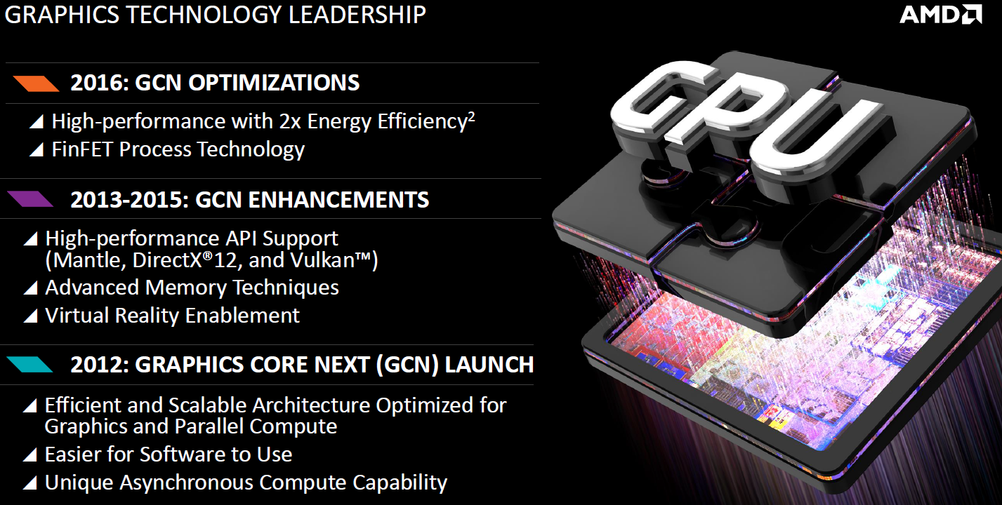
What is noteworthy is that this year year AMDs GCN turns four years old. Previously AMD has never used one ISA [instruction set architecture] for over four years. AMD introduced three generations of its TeraScale architectures over four years (in 2006 2010), each time bringing major improvements. GCN has also evolved significantly since late 2011 and it looks like AMD wants to continue developing generations of GCN-based GPUs.
While AMDs latest Fiji graphics processor based on the third iteration of GCN looks competitive against its rivals, it should be noted that Nvidia has introduced two major architectures (Kepler and Maxwell) since 2012 and plans to unveil Pascal next year.
While architectural innovation may be relatively slow and take time, it should be noted that AMD needs to actually introduce more than one new graphics processor a year, otherwise its lineup will largely consist of outdate GPUs, which will result in further loss of market share.
http://www.kitguru.net/components/gr...-architecture/
Vai ser interessante acompanhar como a AMD tenciona manter-se na linha da frente ou competitiva face ao "Pascal" da nVidia, sendo que a arquitetura continua a ser a mesma e os cortes no R&D estão já a ser feitos.

User Tag List
 Likes: 0
Resultados 16 a 30 de 1047
Tópico: AMD Radeon R7/R9 400
-
13-08-15, 13:39 #16Tech Ubër-Dominus


- Registo
- Nov 2013
- Local
- City 17
- Posts
- 30,121
- Likes (Dados)
- 0
- Likes (Recebidos)
- 2
- Avaliação
- 1 (100%)
- Mentioned
- 0 Post(s)
- Tagged
- 0 Thread(s)
-
21-08-15, 13:05 #17Tech Ubër-Dominus
- Registo
- Nov 2013
- Local
- City 17
- Posts
- 30,121
- Likes (Dados)
- 0
- Likes (Recebidos)
- 2
- Avaliação
- 1 (100%)
- Mentioned
- 0 Post(s)
- Tagged
- 0 Thread(s)
AMDs Greenland GPU May Feature Up To 32 GB of HBM2 Memory Around 15-18 Billion Transistors, Two New GPUs Leaked
It has been four years since the GPU industry saw its first 28nm fabricated product in the form of Tahiti from AMD. Since Tahiti, both AMD and NVIDIA have been stuck on the 28nm node offering little architectural and design changes. While NVIDIA managed to release two new families (Kepler and Maxwell) on the 28nm node, AMD had to stick with their GCN architecture and offered just three new chips after their 7000 series cards in the mainstream and performance oriented lineup that include Tonga, Hawaii and Fiji. With the arrival of the latest FinFET node imminent, AMD is ready to introduce their latest and most beefiest design to date in the form of Greenland GPU in 2016, whose alleged details have made their way on the net.

AMD Greenland GPU May Feature Up To 32 GB GB HBM2 Memory and 18 Billion Transistors
Straight from TweakTown, the latest reports mention the Greenland GPU which has been in the talks for a while now. The latest Arctic Islands family of graphics cards will include the Greenland GPU and fall inside AMDs Radeon 400 series graphics lineup (or AMD might just give it a special name like they did with Fiji). Reports of the Greenland GPU first arrived several months back (prior to the launch of Fury X) where it was revealed that AMD might be preparing a new chip codenamed Greenland but never really revealed the true nature of it. The first report also mentioned that the Greenland GPU will be integrated on APUs with HBM2 memory but now it makes sense as to what the chip was made for. Just a few weeks back, we covered in an article that Greenland would not only become the flagship chip of the stack, but also the most scalable chip AMD will ever produce.

Image Credits: FudzillaAMDs Fiji GPU has shown what is achievable with HBM as it can be incorporated on designs ranging from Fury X, Fury X2, Radeon R9 Nano and even two Fiji chips inside the Quantum PC (which unfortunately will never be made available to consumers). With Greenland, FinFET and HBM2, AMD is aiming towards both the discrete and APU market. An HPC APU design has already made its round and AMD has officially confirmed that they plan to launch a server class APU featuring TFlops of performance. This HBM powered HPC APU will pack the Greenland GPU, several Zen cores, a 100 GB/s interconnect and several GBs of DDR4 memory. This HPC APU is planned for launch in 2017 timeframe and pack 4.0+ TFlops of performance while AMDs current FirePro S9170 accelerator has 2.62 TFlops of performance. While Fiji isnt geared for HPC purposes, a 4.0 TFlops class APU is indeed a marvel of engineering.
So coming back to the discrete part which is also entirely related to the APU part, the rumors not mention that the Greenland GPU will feature around 15-18 billion transistors which falls in line with NVIDIAs Pascal GPU that is going to end up with more than 17 Billion transistors and is based on the FinFET process to, featuring up to 32 GB of HBM2 memory. Now both NVIDIA and AMD have waited a long time to make transition over to a smaller process node. Their current chips are the largest GPUs ever produced in terms of sheer size and overall transistor count (GM200 and Fiji XT). On their Financial Analyst Day, AMD mentioned that their next GCN based cards will feature 2x the energy efficiency over the current GCN iteration. Since FinFET offers up to 90% more transistor density, the 17-18 billion transistors on NVIDIAs and AMDs chip sound completely possible. AMD is expected to offer a completely new GCN architecture with Greenland with a new Instruction Set Architecture or ISA. It has been mentioned that AMD has spent the last two years developing the Greenland GPU and they just recently taped it out.

The performance of next generation graphics cards is indeed going to shake things up. Currently, we see the integrated graphics processors from Intel and AMD closing up on entry level discrete cards but when FinFET comes, we will once again see entry level cards featuring twice or more performance. AMD is planning to incorporate just as much HBM2 memory as NVIDIAs professional and high-end solutions with up to 32 GB of VRAM. The consumer oriented parts will stick with 8-16 GB but the more high-end professional cards will get insane amounts of HBM2 with speeds of 1 TB/s. Technically speaking, both AMD and NVIDIA GPUs sound same in specifications but the ultimate decider would be the price, performance and total efficiency of these cards.
AMD Arctic Islands (Radeon 400 Series) Baffin and Ellesmere Leaked
Two more chips from the Arctic Islands have been tipped by Kitguru which include Baffin and Ellesmere. Now its kind of funny that although these two Islands are found in the north of Canada, they dont essentially fall in the Arctic Islands but rather in the Canadian Islands. Only Greenland is so far the only confirmed GPU that falls in the Arctic Islands so we arent exactly sure whether these codenames can be confirmed right now but AMD does choose names from different Islands, close to each other. For instance, we get to see both Caribbean Islands in the Radeon 300 (Antigua, Trinidad, Tobago, Grenada) and then we see Fiji which isnt a part of the same Islands. These two chips are mainstream and entry level GPUs featuring the latest GCN core design. No more details are yet known but we will sure keep you updated as new information arrives.
GPU Family AMD Arctic Islands NVIDIA Pascal
GPU Family AMD Arctic Islands NVIDIA Pascal GPU Name AMD Greenland NVIDIA GP100 GPU Process 16/14 FinFET 16/14nm FinFET GPU Transistors 15-18 Billion ~17 Billion HBM Memory (Consumers) 4-16 GB (SK Hynix) HBM2 2-16 GB (SK Hynix/Samsung)
HBM2HBM Memory (Professional) 32 GB (SK Hynix) HBM2 32 GB (SK Hynix/Samsung) HBM2 HBM2 Bandwidth 1 TB/s (Peak) 1 TB/s (Peak) Graphics Architecture GCN 2.0? (New ISA) Next-CUDA (Compute Oriented) Successor of (GPU) Fiji (Radeon 300/Fury) GM200 (Maxwell)
-
21-08-15, 13:16 #18O Administrador
- Registo
- Mar 2013
- Local
- Multiverso
- Posts
- 17,814
- Likes (Dados)
- 74
- Likes (Recebidos)
- 156
- Avaliação
- 31 (100%)
- Mentioned
- 31 Post(s)
- Tagged
- 0 Thread(s)
Boas!
Tendo em conta que a largura de banda deixa de ser um limite, passa agora a contar o gpu e as optimizações que o mesmo tenha.
Eficiência da arquitectura e claro o custo.
Para mim a chave para o sucesso será ter mais por menos preço que o concorrente... quem vender mais barato ganha o cliente.
Cumprimentos,
LPCMy Specs: .....

CPU: AMD Ryzen 7 5800X3D :-: Board: MSI B550M BAZOOKA :-: RAM: 64 GB DDR4 Kingston Fury Renegade 3600 Mhz CL16 :-: Storage: Kingston NV2 NVMe 2 TB + Kingston NV2 NVMe 1 TB
CPU Cooling Solution: ThermalRight Frost Commander 140 Black + ThermalRight TL-C12B-S 12CM PWM + ThermalRight TL-C14C-S 14CM PWM :-: PSU: Corsair HX 1200 WATTS
Case: NZXT H6 FLOW :-: Internal Cooling: 4x ThermalRight TL-C12B-S 12CM PWM + 4x ThermalRight TL-C14C-S 14CM PWM
GPU: ASUS TUF AMD RADEON RX 7900 XTX - 24 GB :-: Monitor: BenQ EW3270U 4K HDR
-
27-08-15, 07:59 #19Tech Ubër-Dominus
- Registo
- Nov 2013
- Local
- City 17
- Posts
- 30,121
- Likes (Dados)
- 0
- Likes (Recebidos)
- 2
- Avaliação
- 1 (100%)
- Mentioned
- 0 Post(s)
- Tagged
- 0 Thread(s)
AMD Next Generation ‘Arctic Islands’ Graphic Cards Will Be Manufactured on the 16nm FinFET+ Node From TSMC
So it looks like we have the first independent confirmation about AMD Radeon’s exact node. TSMC will be manufacturing the next generation AMD graphic cards (Arctic Islands and Greenland) on their 16nm FinFET node – something that was pretty much expected. It would appear however, that AMD will be reverting to Global Foundry’s 14nm FinFET process for its Zen based processors (via KitGuru). While this aspect of the news (Zen) is also not really surprising, I would urge users to take it with a grain of salt, since it is very clearly not confirmed yet.
AMD Greenland graphics to be manufactured on the same node as the Pascal flagship – Zen possibly contracted to Global Fondries Not an official poster. @WCCFTech
One of the major problems (in my humble opinion) for graphic card manufacturers is that foundries like TSMC usually allot high priority to clients like Apple. This means that they get the first spot in a queue and the first try at the goods even after a specific node has matured to the point it can be used for high performance ASICs (which mobile SOCs do not really qualify as). TSMC lost quite a bit of share of Apple’s A9 chips to Samsung Electronics and while it has retained a portion of the order, Qualcomm has decided to deal exclusively with Samsung this time. This reduction in clients and therefore the bump in the priority queue might (read: possible, not probable) translate to the next gen GPUs coming just a bit earlier.
TSMC’s 16FF+ (FinFET Plus) technology can provide above 65 percent higher speed, around 2 times the density, or 70 percent less power than its 28HPM technology. Comparing with 20SoC technology, 16FF+ provides extra 40% higher speed and 60% power saving. By leveraging the experience of 20SoC technology, TSMC 16FF+ shares the same metal backend process in order to quickly improve yield and demonstrate process maturity for time-to-market value. Now it is the 16FF+ variant that is of specific interest to us – because it is this variant that the AMD and Nvidia will most probably settle for.
TSMC and Nvidia have also confirmed on more than one occasion that the next generation (Pascal) GPUs will be produced on the 16nm FinFET+ node, with initial confirmation dating back approximately 9 months. AMD’s next generation Radeon graphics processor on the other hand, codenamed Arctic Islands, was not (initially) on the official list of products released by TSMC, so while their CEO have confirmed the use of a FinFET node (14/16) the exact specifics had remained to be seen. That particular mystery can now be considered solved since Digitimes reports the future Arctic Islands lineup from AMD will be fabricated on the same process (as always) as Nvidia’s GP100 GPU. Interestingly, there is no word on Zen yet, which might indicate a reversion to Global Foundries as originally stated.
16nm FinFET tech entered into risk production and approached mature yields a while back, and now full fledged production has begun full steam ahead. More than 60 projects are underway, with known products in development including Avago, Freescale, LG, MediaTek, NVIDIA, AMD, Renesas and Xilinx. The list is obviously not exhaustive in nature but it finally includes the two companies our readers are most interested in: AMD and Nvidia. There have been rumors circulating about red and green flagships (namely Greenland and Pascal) with an insane amount of transistors (17-18 Billion) and I must say that unless TSMC has deliberately withheld details about its new process, I find the premise of a ~600mm^2 first generation 16nm FinFET+ product from any company very unlikely.
-
27-08-15, 13:36 #20O Administrador
- Registo
- Mar 2013
- Local
- Multiverso
- Posts
- 17,814
- Likes (Dados)
- 74
- Likes (Recebidos)
- 156
- Avaliação
- 31 (100%)
- Mentioned
- 31 Post(s)
- Tagged
- 0 Thread(s)
Boas!
Hummmm
Gráficas 16nm e cpus a 14nm... Se as arquitecturas vierem boas temos bombas vindas do lado da AMD...
Mais uma vez apenas me preocupa o desespero da empresa em vender e meter os preços altos...
Cumprimentos,
LPCMy Specs: .....
CPU: AMD Ryzen 7 5800X3D :-: Board: MSI B550M BAZOOKA :-: RAM: 64 GB DDR4 Kingston Fury Renegade 3600 Mhz CL16 :-: Storage: Kingston NV2 NVMe 2 TB + Kingston NV2 NVMe 1 TB
CPU Cooling Solution: ThermalRight Frost Commander 140 Black + ThermalRight TL-C12B-S 12CM PWM + ThermalRight TL-C14C-S 14CM PWM :-: PSU: Corsair HX 1200 WATTS
Case: NZXT H6 FLOW :-: Internal Cooling: 4x ThermalRight TL-C12B-S 12CM PWM + 4x ThermalRight TL-C14C-S 14CM PWM
GPU: ASUS TUF AMD RADEON RX 7900 XTX - 24 GB :-: Monitor: BenQ EW3270U 4K HDR
-
27-08-15, 15:00 #21Master Business & GPU Man

- Registo
- Jan 2015
- Local
- País Campeão Euro 2016
- Posts
- 7,793
- Likes (Dados)
- 0
- Likes (Recebidos)
- 1
- Avaliação
- 41 (100%)
- Mentioned
- 0 Post(s)
- Tagged
- 0 Thread(s)
A mim não me preocupa muito os preços. Se for bom, a malta compra. Se for o melhor, a malta esgota. Post Original de LPC

O problema da AMD está mais no timming do que nos preços. Se eles lançarem essa coisa no final de 2016, já a Nvidia os cilindrou a meio do ano.
Como já falamos, se a Fury tivesse saído em Janeiro ao preço que saiu em Agosto, só havia a Titan X no mercado a +400eur...Mesmo que a 980Ti viesse depois e ligeiramente melhor como é, teria de conquistar terreno perdido. Conquistar terreno perdido é correr atrás do prejuizo. E a AMD é perita nisso....Ideias sem Nexo e Provas do Tráfico de Hardware
"que personifica o destino, equilíbrio e vingança divina." Dejá vú. Que cena!
-
18-10-15, 19:44 #22Tech Ubër-Dominus
- Registo
- Nov 2013
- Local
- City 17
- Posts
- 30,121
- Likes (Dados)
- 0
- Likes (Recebidos)
- 2
- Avaliação
- 1 (100%)
- Mentioned
- 0 Post(s)
- Tagged
- 0 Thread(s)
AMD: Our Next Generation (Arctic Islands) GPUs will offer Double the Performance Per Watt of the Current Generation
It looks like the GPUs in 2016 are going to be a major step up from current gen, because we keep on hearing about performance basically doubling, thanks to the transition to the smaller node. There have been reports in the past about Nvidia’s Pascal having 17 Billion transistors (more than twice as many as the Maxwell flasghip) and even now at AMD’s earnings call, Lisa Su stated that the next generation AMD graphic cards will double the performance per watt delivered by the current generation (Fiji) lineup.
AMD’s Arctic Islands lineup will offer atleast ‘double the performance per watt’ of Fiji processorsNot an official poster. @WCCFTech
While it has been implied in the past that the performance jump is going to be enormous, this is one of the few times where the company has explicitly mentioned just how big the jump is going to be. Lisa Su made the following statement on the recently held earnings call for the results of the third quarter, year ended 2015:
“We are also focused on delivering our next generation GPUs in 2016 which is going to improve performance per watt by two times compared to our current offerings, based on design and architectural enhancements as well as advanced FinFET products process technology.” – Lisa Su, AMDThe alleged codename of the Arctic Islands’ flagship is ‘Greenland’ and if what AMD says is true (and there is no reason for it to not be just that) we are looking at a 100% increase in performance over Fiji. But just what exactly does that translate to in terms of numbers? Using what we know about the FinFET process, we can arrive at a tentative answer.
While Nvidia is confirmed to be on the 16nm FinFET+ node from TSMC, the same cannot be said about AMD. We do however, have more authentic reports about AMD being on the 16FF+ node as opposed to 14nm FinFET. So if we are to assume that the same is true for AMD, then it is going to adhere to the same rules as Nvidia’s next process. Here is an official summary of the 16FF+ node from TSMC official:
TSMC’s 16FF+ (FinFET Plus) technology can provide above 65 percent higher speed, around 2 times the density, or 70 percent less power than its 28HPM technology. Comparing with 20SoC technology, 16FF+ provides extra 40% higher speed and 60% power saving. By leveraging the experience of 20SoC technology, TSMC 16FF+ shares the same metal backend process in order to quickly improve yield and demonstrate process maturity for time-to-market value.Fiji GPU has a total of 4096 stream processors and 8.9 Billion transistors and the die size is 596mm^2. So for double the performance, we are looking around 18 Billion transistors for the Greenland (Arctic Islands) chip. Ofcourse, if the die size is ~500mm^2 initially then anything in the range of 15 Billion transistors goes. For the ~500mm assumption, after accounting for performance increases via architectural improvements, a gain of 66%+ (anything between 70-80% realistically) can be expected. While that is not a full 100%, it is close enough. Ofcourse we have no idea what the stream processor size will be, so attempting to reverse engineer the exact core count would be an exercise in futility. It is a safe bet however that the number would be somewhere around the 8192 mark for a ~600mm die or around the 6784 mark for the ~500mm die (plus minus a few multiples of 128).
The GM200 on the other hand, has 8 Billion transistors, so double the density would yield around 16 Billion transistors for a ~600mm chip according to TSMC specs assuming the transistor specifications remain the same. If we are to assume a ~500mm^2 chip for the initial 16nm FinFET+ run then the transistor count would be roughly 14 Billion transistors. If the rumor about Nvidia bringing 17 Billion transistors to the table is true, then either TSMC can manage a ~600mm^2 chip right off the bat, or, Nvidia’s next generation Pascal GPUs will have a new transistor-to-core ratio and design (improbable).
While the fact that TSMC is using the 20nm back end process helps in the claims of a ~600mm^2 die, I myself, have difficulty believing that these companies will launch with such huge dies. It is possible that competition might force them to do so, but in my opinion, the probability of an initial ~500mm^2 die is much greater. At any rate, we are going to have an absolutely amazing showdown in 2016, with the first full fledged, 4K @60fps monsters landing in the DirectX 12 arena. It is most definitely a good time to be a PC gamer.
-
18-10-15, 22:06 #23Tech Membro
- Registo
- Mar 2013
- Local
- C.Branco
- Posts
- 2,326
- Likes (Dados)
- 0
- Likes (Recebidos)
- 0
- Avaliação
- 0
- Mentioned
- 0 Post(s)
- Tagged
- 0 Thread(s)

Venham de lá esses yields em força, que tá na hora de recuperar mercado. Aliás, já passa. XD
-
18-10-15, 22:29 #24O Administrador
- Registo
- Mar 2013
- Local
- Multiverso
- Posts
- 17,814
- Likes (Dados)
- 74
- Likes (Recebidos)
- 156
- Avaliação
- 31 (100%)
- Mentioned
- 31 Post(s)
- Tagged
- 0 Thread(s)
Boas! Post Original de MAXLD
APOIADO!
Para ontem já é tarde!
Cumprimentos,
LPCMy Specs: .....
CPU: AMD Ryzen 7 5800X3D :-: Board: MSI B550M BAZOOKA :-: RAM: 64 GB DDR4 Kingston Fury Renegade 3600 Mhz CL16 :-: Storage: Kingston NV2 NVMe 2 TB + Kingston NV2 NVMe 1 TB
CPU Cooling Solution: ThermalRight Frost Commander 140 Black + ThermalRight TL-C12B-S 12CM PWM + ThermalRight TL-C14C-S 14CM PWM :-: PSU: Corsair HX 1200 WATTS
Case: NZXT H6 FLOW :-: Internal Cooling: 4x ThermalRight TL-C12B-S 12CM PWM + 4x ThermalRight TL-C14C-S 14CM PWM
GPU: ASUS TUF AMD RADEON RX 7900 XTX - 24 GB :-: Monitor: BenQ EW3270U 4K HDR
-
21-10-15, 17:38 #25Tech Ubër-Dominus
- Registo
- Nov 2013
- Local
- City 17
- Posts
- 30,121
- Likes (Dados)
- 0
- Likes (Recebidos)
- 2
- Avaliação
- 1 (100%)
- Mentioned
- 0 Post(s)
- Tagged
- 0 Thread(s)
AMD Updating Entire Graphics Line-Up In The Coming Quarters – 14nm/16nm Arctic Islands GPUs Arriving In 2016
AMD’s President and CEO Lisa Su confirmed that the company plans to update its entire AIB and OEM graphics portfolio over the coming quarters. A revelation which took place at the company’s Q3 2015 earnings teleconference as Su affirmed the company’s commitment to graphics innovation and asserted that traditional graphics markets are still a major focus for the company. Su disclosed that AMD made good progress in growing share in traditional graphics markets in Q3 2015 and has plans in place to continue this growth over a number of quarters.

Su pointed out that the recent formation of a vertical business unit that encompasses all things graphics inside AMD dubbed the Radeon Technologies Group was driven principally by an objective to strengthen the company’s competitive position in the traditional graphics markets, such as the add-in-board channel and OEM as well as accelerate growth in emerging markets such as virtual reality.
Lisa Su – Advanced Micro Devices, Inc. – President, CEOAMD To Update Its Entire Graphics Line-Up With 14nm/16nm FinFET “Arctic Islands” GPUs
We successfully executed many of our near-term tactical priorities in the third quarter, while also taking several key steps as a part of our longer-term strategy to focus AMD on delivering great products, driving deeper customer relationships, and simplifying our business. Highlights include delivering strong double-digit sequential revenue growth in each of our business segments; expanding our product portfolio with the introduction of several new APUs and GPUs that improve our competitive positioning in key markets; forming the Radeon Technologies Group to bring a vertical focus to our graphics business and help strengthen our performance in traditional graphics markets, while simultaneously establishing leadership initiatives in emerging — immersive computing markets, like virtual and augmented reality.Joe Moore – Morgan Stanley – AnalystSu confirmed that AMD is set to update its entire graphics portfolio in 2016. The new family of GPUs will feature significant architectural enhancements as well as cutting edge FinFET process technology to deliver twice the performance per watt of AMD’s current graphics offerings.
You have had a nice sequential quarter, but I still have your GPU business down quite a lot year over year. Now that you have products that are more competitive in the enthusiast segment, can you give us an upper bound of
what you might be able to achieve there? Is there supply constraints that are keeping this small and are you going to be able to regain the levels that you were at a year ago in GPU?
Lisa Su – Advanced Micro Devices, Inc. – President, CEO
Yes, so Joe, I think one quarter is good progress. Now you will have to watch us over a number of quarters regain that graphics momentum.
And when I think about it, relative to the Fury launch we did have some supply constraints in the third quarter. They were — they are largely solved in the fourth quarter, so I don’t think there will be any supply constraints.
I think it’s also fair to say that the graphics portfolio is quite broad, and so you will see us updating the entire portfolio over the coming quarters,
Lisa Su – Advanced Micro Devices, Inc. – President, CEOI should point out right away that AMD does not officially acknowledge the process technology specifics of its next generation GPUs. AMD has two foundry partners that poses FinFET manufacturing technology. Globalfoundries has 14nm 14LPE (Low Power Early/Extreme) and 14LPP (Low Power Performance). TSMC has 16nm 16FF (FinFET) and 16FF+ (FinFET+). 14LPE and 16FF are the early iterations of the technology, while 14LPP and 16FF+ are the refined, higher performance versions of the technology. Despite what the names might suggest, these 14nm and 16nm process technologies actually have nearly identical feature sizes.
We are also focused on delivering our next-generation GPUs in 2016 designed to improve performance per watt by 2X compared to our current offerings, based on design architectural enhancements, as well as advanced FinFET process technology.
AMD’s CEO Lisa Su confirmed that the company’s engineering teams have taped out multiple FinFET designs for both foundries in Q3 2015, but did not go into further detail. However, historical precedent – all GPUs in the company’s history made their debut on a TSMC process technology – as well as numerous reports point towards TSMC’s 16nm FinFET process as being the likely candidate over Globalfoundries’ 14nm for AMD’s next generation graphics chips. While Globalfoundries’ 14nm remains the favorite for the company’s future Zen based CPU and APU designs.

This new family of 16nm GPUs is informally code named “Arctic Islands”. The new family will be based on AMD’s 3rd generation GCN (Graphics Core Next) architecture. Interestingly — despite the existence of three+ different iterations of GCN namely GCN 1.0 ( HD 7000 series ) , GCN 1.1 ( R9 290 series) , GCN 1.2 ( R9 285 and 380) and Fiji ( R9 Fury X, R9 Fury and R9 Nano) which is based on an updated GCN 1.2 design — according to AMD there have only been two generations of GCN so far. With the next major iteration coming next year in the form of the “Arctic Islands” family of graphics chips.
This graphics architecture will power everything from next generation mobile and desktop GPUs, APUs as well as semi-custom. There’s also strong evidence to suggest that Nindendo’s next generation gaming device “Nintendo NX” – which is coming next year – will be powered by an AMD semi-custom SOC. Making it a very likely candidate to feature AMD’s 3rd generation “Arctic Islands” GCN architecture.
The flagship GPU in the family has been numerously reported to be code named “Greenland“. Which is set to be AMD’s most powerful and most advanced graphics chip to date. In addition to being build on an advanced FinFET manufacturing process – likely 16FF+ at TSMC, the same for Nvidia’s Pascal – the Arctic Islands family will feature second generation High Bandwidth Memory Technology and as mentioned earlier an updated 3rd generation GCN architecture. These -16nm, HBM2 and GCN3- are going to be the three main performance and power efficiency driving features. Greenland specifically is rumored to feature up to 18 billion transistors and 32GB of second generation HBM with 1TB/s of memory bandwidth. Making it the largest ever graphics engine conceived by the company, at approximately twice the transistor count of the AMD’s current flagship “Fiji”.
WCCFTech Year Process Flagship GPU Product Memory Bandwidth Southern Islands 2012 28nm Tahiti HD 7970 3GB GDDR5 264GB/s Volcanic Islands 2013 28nm Hawaii R9 290X 4GB GDDR5 320GB/s Pirate/Caribbean Islands 2015 28nm Fiji R9 Fury X 4GB HBM1 512GB/s Arctic Islands 2016 14/16nm FinFET Greenland ? ?GB HBM2 1TB/s
-
21-10-15, 21:52 #26Master Business & GPU Man
- Registo
- Jan 2015
- Local
- País Campeão Euro 2016
- Posts
- 7,793
- Likes (Dados)
- 0
- Likes (Recebidos)
- 1
- Avaliação
- 41 (100%)
- Mentioned
- 0 Post(s)
- Tagged
- 0 Thread(s)
Estranho a AMD falar em eficiencia energetica, depois de ter destilado com benchmarks de 7990's, pondo a fonte em altas.
A promessa está a valer 50% de mercado.lol. Bora AMD! No mês passado já era tarde!!Ideias sem Nexo e Provas do Tráfico de Hardware
"que personifica o destino, equilíbrio e vingança divina." Dejá vú. Que cena!
-
23-10-15, 15:50 #27Tech Ubër-Dominus
- Registo
- Nov 2013
- Local
- City 17
- Posts
- 30,121
- Likes (Dados)
- 0
- Likes (Recebidos)
- 2
- Avaliação
- 1 (100%)
- Mentioned
- 0 Post(s)
- Tagged
- 0 Thread(s)
AMD R 400 Series Ellesmere And Baffin “Arctic Islands” GPUs Taped Out, To Enter Production In 2016
AMD’s next generation “Arctic Islands” family of FinFET GPUs has been subject to a number of leaks this year. One of which indicated that the family contains three new GPUs, code named Greenland, Ellesmere and Baffin. Today we’re not only confirming that this is information is in fact accurate but that both Ellesmere and Baffin have in fact taped out and are awaiting commencement of FinFET process volume production to kick off next year.
AMD has also managed to secure a major OEM design win with both “Ellesmere” and “Baffin” GPUs a source with knowledge of AMD’s roadmap confirmed to WCCFTech. Greenland will be AMD’s next generation flagship GPU, while Ellesmere and Baffin will address the performance and mainstream segments of the market. The Arctic Islands family will debut with the three aforementioned GPUs in a variety of SKUs which will address the entire discrete GPU market top to bottom. We’ve seen this three GPU strategy before with AMD’s first 28nm GPUs code named “Southern Islands” in the form of the HD 7900 series, HD 7800 series and HD 7700 series.
AMD Arctic Islands Family Entering Production Next Year
Yesterday we detailed AMD’s plans to update the entire graphics line-up over “the coming quarters” with a new set of products that have “2X the performance per watt” of AMD’s current GPUs.
Lisa Su – Advanced Micro Devices, Inc. – President, CEO – Q3 2015 Earnings Teleconference
I think it’s also fair to say that the graphics portfolio is quite broad, and so you will see us updating the entire portfolio over the coming quarters,Lisa Su – Advanced Micro Devices, Inc. – President, CEO – Q3 2015 Earnings TeleconferenceDespite the existence of three+ different iterations of GCN namely GCN 1.0 ( HD 7000 series ) , GCN 1.1 ( R9 290 series) , GCN 1.2 ( R9 285 and 380) and Fiji ( R9 Fury X, R9 Fury and R9 Nano) which is based on an updated GCN 1.2 design; according to AMD’s Chief Technology Officer Mark Papermaster there have only been two generations of GCN so far. With the next major iteration – 3rd generation – coming next year in the form of the “Arctic Islands” family of graphics chips.
We are also focused on delivering our next-generation GPUs in 2016 designed to improve performance per watt by 2X compared to our current offerings, based on design architectural enhancements, as well as advanced FinFET process technology.
Arctic Islands will feature three major improvements over AMD’s current current R 300 series and Fury series line-up. These include second generation HBM, next generation GCN architecture as well as a more advanced 14/16nm FinFET manufacturing process. The three of which will define the performance and power efficiency characteristics of the Arctic Islands family.

It was confirmed back in August that AMD is in fact one of TSMC’s clients for the 16nm node. That, in addition to historical precedent and a number of reports indicate that AMD will indeed manufacture its next generation GPUs using TSMC’s 16nm process. TSMC’s 16nm FinFET process node offers double the transistor density of current 28nm technology as well as faster switching speeds – which translate to higher clock speeds – and finally significantly lower power consumption per transistor. So we’re looking at larger graphics engines than AMD’s current line-up with faster clock speeds and significantly better power efficiency.
TSMC.comIt will be interesting to see how things shape up next year with Nvidia’s Pascal GPUs which will also be produced on TSMC’s 16nm FinFET process and feature second generation High Bandwidth Memory. When exactly Pascal and Arctic Islands GPUs will be released and how much they’re going to cost will depend almost entirely on 16nm production yields and volumes. But so far this is shaping up to be one of the biggest performance and power efficiency boosts we’re going to see from a new generation of graphics cards in a long while.
TSMC’s 16FF+ (FinFET Plus) technology can provide above 65 percent higher speed, around 2 times the density, or 70 percent less power than its 28HPM technology. Comparing with 20SoC technology, 16FF+ provides extra 40% higher speed and 60% power saving. By leveraging the experience of 20SoC technology, TSMC 16FF+ shares the same metal backend process in order to quickly improve yield and demonstrate process maturity for time-to-market value.
WCCFTech Year Process Flagship GPU Product Memory Bandwidth Southern Islands 2012 28nm Tahiti HD 7970 3GB GDDR5 264GB/s Volcanic Islands 2013 28nm Hawaii R9 290X 4GB GDDR5 320GB/s Pirate/Caribbean Islands 2015 28nm Fiji R9 Fury X 4GB HBM1 512GB/s Arctic Islands 2016 14/16nm FinFET Greenland ? ?GB HBM2 1TB/s
-
26-10-15, 16:15 #28Tech Ubër-Dominus
- Registo
- Nov 2013
- Local
- City 17
- Posts
- 30,121
- Likes (Dados)
- 0
- Likes (Recebidos)
- 2
- Avaliação
- 1 (100%)
- Mentioned
- 0 Post(s)
- Tagged
- 0 Thread(s)
Leaked Slide Suggests AMD and NVIDIA Will Both Use GDDR5X
Noticia:
We have previously reported the rumours that Nvidia was planning to use GDDR5X on their upcoming Pascal graphics cards, a rumour that not everyone bought right away. But there are quite a few reasons that we could see this happen and the newest leak seems to support this.
Last time it was a German site that leaked the GDDR5X information and this time we get news from a Russian outlet that got their hands on what looks like leaked slides from Micron of the upcoming GDDR5x memory. The site also suggests that this won’t be limited to only Nvidia, but that AMD also will want to get on board and use this type of memory on some of their graphics cards next year.
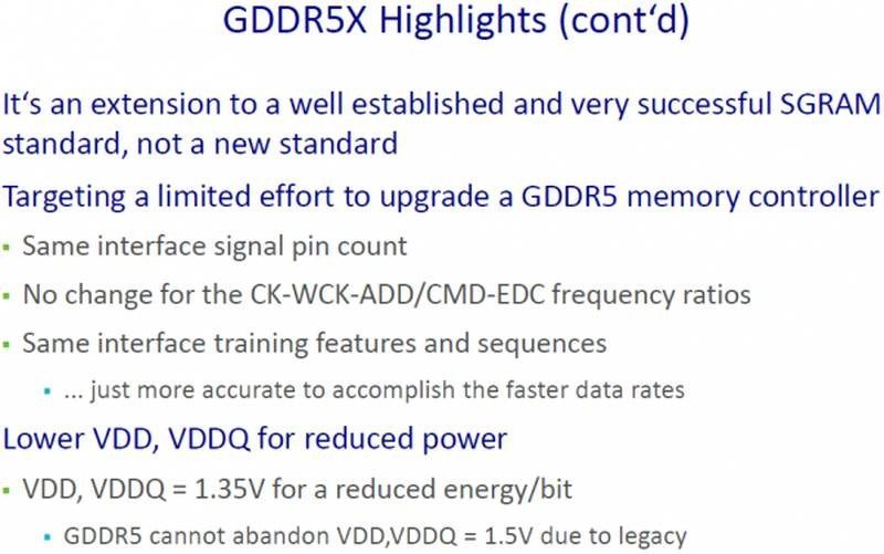
HBM, and HBM2 might be very exciting and be the next mainstream graphics memory, but it is still a costly one to produce and the production is also limited. This leaves room for the next GDDR5 standard to make its entry. GDDR5X offers double the data-rate per memory access of 64 byte/access compared to 32 byte/access of the current GDDR5 standard. Where current GDDR5 tops out at around 7Gbps, the new standard will initially offer 10-12 Gbps with a later goal to achieve 16 Gbps.
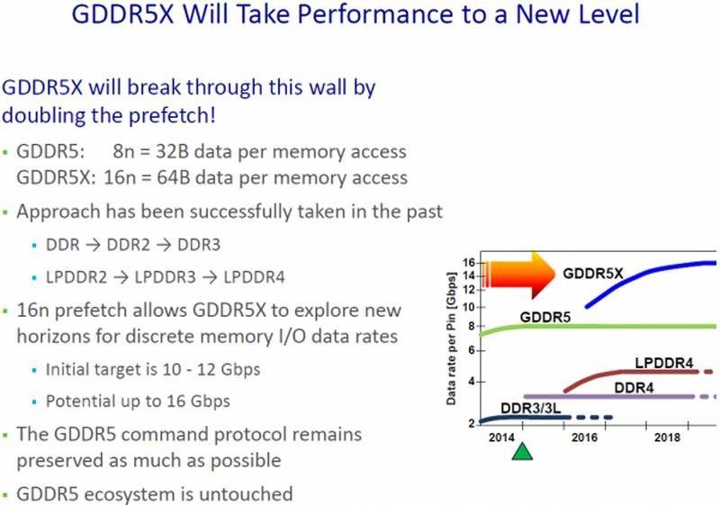
The implementation of the new memory should be relatively easy and cheap for manufacturers as the new chips will retain the same pin layout. With all this information, we can assume that HBM will be reserved for the top-tier graphics cards for the foreseeable future while GDDR5x will breath more power into mid-level and entry-level cards and allow them to perform better at the ever-increasing resolutions.
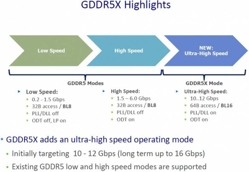
http://www.eteknix.com/slide-leak-su...ll-use-gddr5x/
-
10-11-15, 14:00 #29Tech Ubër-Dominus
- Registo
- Nov 2013
- Local
- City 17
- Posts
- 30,121
- Likes (Dados)
- 0
- Likes (Recebidos)
- 2
- Avaliação
- 1 (100%)
- Mentioned
- 0 Post(s)
- Tagged
- 0 Thread(s)
AMD investing heavily to "win the graphics battle" next year
Noticia:AMD has been going through a challenging time, clearly illustrated by its most recent set of quarterly results, headlined by a $197 million loss. That result marked AMD's fourth straight quarter of losses. At the time of those results, just a under a month ago, AMD CEO Dr Lisa Su released an upbeat statement highlighting revenue growth trends, a focus upon company strengths, and upon long term goals.
Now another senior AMD exec is heralding a turnaround, a confident return to profitability for AMD. AMD's EMEA component sales manager Neil Spicer spoke to CRN yesterday, echoing the CEO's drum beat of sticking to company strengths, remaining true to its 'core ethos'.

AMD's EMEA component sales manager Neil Spicer"I believe we are working with exactly the right customers, and over the last few years we have become much simpler to execute and do business with," said Spicer. Looking forward Spicer said that AMD has to focus on AMD's historical strengths of graphics and in making chips that are attractive enough to be included in the Windows 10 upgrade cycle.
Winning the graphics battle
AMD is going to "invest heavily," asserted Spicer with the purpose of "winning the graphics battle with gaming" and more. The next-generation Zen processor was touched upon in the CRN interview. This processor will help AMD compete in the high end desktop and server markets, thought Spicer.
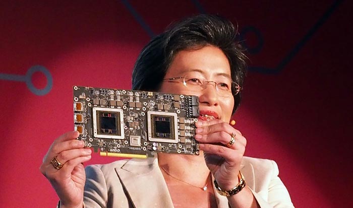
AMD CEO Dr Lisa Su holds aloft a Radeon R9 Fury X2Overall it looks like AMD has confidently set sail to deliver on its promises in 2016. Let's just hope it can reach safe harbour by returning to profitability and secure its future, and the future of competition, in the PC CPU and GPU markets.
http://hexus.net/business/news/compo...tle-next-year/
Será que vai mesmo ganhar?
Depois de várias derrotas sucessivas nestas ultimas gerações, era bom ver novamente a AMD competitiva ou até melhor face ao Pascal da nVidia.
-
10-11-15, 14:27 #30Tech Membro
- Registo
- Mar 2013
- Local
- C.Branco
- Posts
- 2,326
- Likes (Dados)
- 0
- Likes (Recebidos)
- 0
- Avaliação
- 0
- Mentioned
- 0 Post(s)
- Tagged
- 0 Thread(s)
Esperemos que não passe apenas de conversa para manter algum moral nos investidores/accionistas, e que realmente se concretize. Zen, low level APIs, e HBM são basicamente as grandes oportunidades de ter algo que realmente faça a diferença e suba a reputação da empresa.
Se não for lá com isso, então só mesmo se for o Zézé Camarinha a comandar a nVidia nos próximos anos...


 Responder com Citação


Informação da Thread
Users Browsing this Thread
Estão neste momento 1 users a ver esta thread. (0 membros e 1 visitantes)
 Regras
São agora 22:49.
 User Alert System provided by
Advanced User Tagging v3.3.0 (Lite) -
vBulletin Mods & Addons Copyright © 2024 DragonByte Technologies Ltd.
User Alert System provided by
Advanced User Tagging v3.3.0 (Lite) -
vBulletin Mods & Addons Copyright © 2024 DragonByte Technologies Ltd.
Feedback Buttons provided by Advanced Post Thanks / Like (Lite) - vBulletin Mods & Addons Copyright © 2024 DragonByte Technologies Ltd.
Portugal-Tech 2012-24 | Todos os direitos reservados! Alojamento Powered by: Trignosfera
Powered by vBulletin® Version 4.2.5 Alpha 3
Copyright © 2024 vBulletin Solutions, Inc. All rights reserved.
Copyright © 2024 vBulletin Solutions, Inc. All rights reserved.
Feedback Buttons provided by Advanced Post Thanks / Like (Lite) - vBulletin Mods & Addons Copyright © 2024 DragonByte Technologies Ltd.
Portugal-Tech 2012-24 | Todos os direitos reservados! Alojamento Powered by: Trignosfera
Bookmarks