

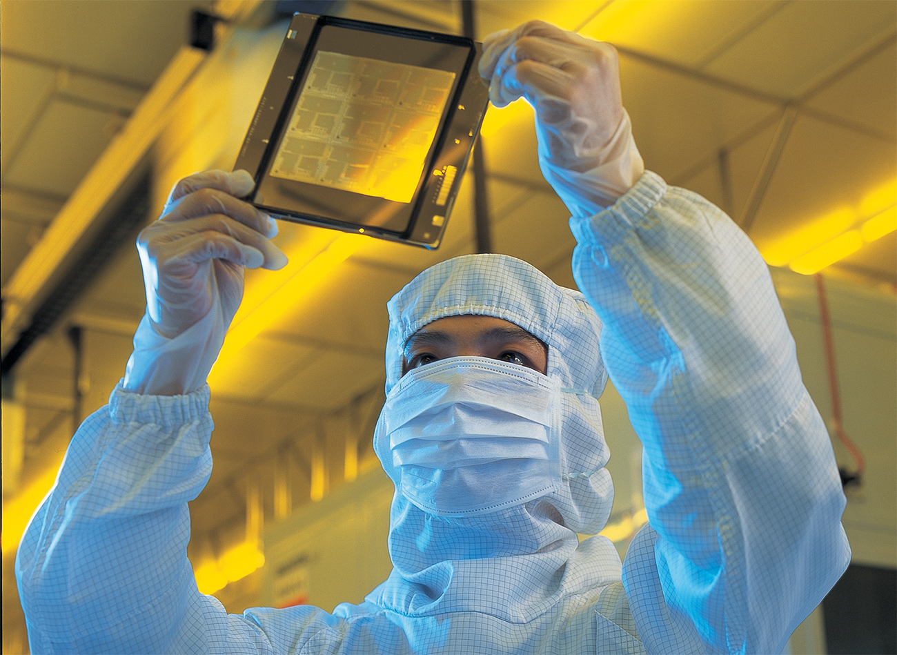
TSMC: We will start risk production of 7nm chips in 2017
Noticia:Taiwan Semiconductor Manufacturing Co. remains optimistic about its abilities to make chips using thinner process technologies going forward. Last week the company said that it would start risk production of integrated circuits using its 7nm process technology in 2017. Mass production of commercial 7nm products will likely begin in 2018, about a year after the start of risk production.
TSMC started to develop its 7nm fabrication technology in early 2014. By now, the company has designed the majority of key elements of the new manufacturing process and even has begun its 7nm design and technology collaboration activity with several of its major customers. Such collaborations help to ensure that TSMC’s fabrication processes deliver what its clients need.
“Our 7nm technology developments today are well in progress,” said Mark Liu, TSMC president and co-CEO, during the company’s conference call with investors and financial analysts last week. “TSMC’s 7nm technology will leverage most of the tools used in 10nm, in the meantime achieve a new generation of technology value to our customers. The 7nm technology risk production date is targeted at early 2017.”
According to TSMC, it will continue to use immersion tools with innovative multiple patterning techniques at 7nm node and is evaluating usage of extreme ultraviolet (EUV) lithography to reduce complexity and manufacturing costs.
“The EUV technology provides not only some cost benefit, but also simplify the process,” added Mr. Liu. “That means you can replace multiple layers with one layer that helps your yield improvement. So there is opportunity both in quality and cost always exist so long as EUV’s productivity comes to the threshold point.”
TSMC admits that EUV lithography is still in the engineering mode and is years away from mass adoption. As a result, it is possible that the company’s 10nm process technology will not get an EUV option at all.
http://www.kitguru.net/components/gr...chips-in-2017/
A TSMC é primeira a revelar planos para os 7nm, mesmo antes da Intel.

User Tag List
 Likes: 0
Resultados 61 a 75 de 134
-
21-04-15, 14:30 #61Tech Ubër-Dominus


- Registo
- Nov 2013
- Local
- City 17
- Posts
- 30,121
- Likes (Dados)
- 0
- Likes (Recebidos)
- 2
- Avaliação
- 1 (100%)
- Mentioned
- 0 Post(s)
- Tagged
- 0 Thread(s)
-
21-04-15, 17:25 #62Moderador

- Registo
- Feb 2013
- Local
- Santo Tirso
- Posts
- 12,672
- Likes (Dados)
- 30
- Likes (Recebidos)
- 208
- Avaliação
- 4 (100%)
- Mentioned
- 7 Post(s)
- Tagged
- 0 Thread(s)
A questão é se conseguem cumprir, ou se vamos ter algo parecido com os 16nm.
Ryzen R5 3700X / Noctua NH-D15 / B550 AORUS ELITE V2 / Cooler Master H500 Mesh / 16Gb DDR4 @ 3800mhz CL16 / Gigabyte RTX 2070 Super / Seasonic Focus GX 750W / Sabrent Q Rocket 2 TB / Crucial MX300 500Gb + Samsung 250Evo 500Gb / Edifier R1700BT
-
22-04-15, 15:21 #63Tech Ubër-Dominus
- Registo
- Nov 2013
- Local
- City 17
- Posts
- 30,121
- Likes (Dados)
- 0
- Likes (Recebidos)
- 2
- Avaliação
- 1 (100%)
- Mentioned
- 0 Post(s)
- Tagged
- 0 Thread(s)
Internet of Things will kick-start semi-conductor industry
Noticia:
TSMC sees gold in them thar hills
Internet of Things (IoT) will be the semiconductor industry's next growth driver, according to TSMC president and co-CEO CC Wei.
Wei believes that the healthcare chip market will reach US$6.8 billion in production value in 2017, said Wei. Meanwhile a family home could feature more than 500 smart devices by 2020.
He said that mobile devices have already replaced PCs as the major growth driver of the semiconductor market and in 2014, about 1.88 billion mobile phones were shipped with 1.2 billion of them being smartphones.
Technology is also enabling devices to progress. Taking PC as an example, the penetration rate of the devices has been pushed up thanks to more advanced chip-making technologies, Wei said.
Worldwide semiconductor R&D expenditures were as high as US$56 billion in 2013, with the US semiconductor industry contributing the most at US$33 billion. Taiwan's R&D expenditures for the year came to about an impressive US$5 billion, Wei noted.
Among the industry's top-10 R&D spenders in 2014, two Taiwan-based companies were listed, Wei disclosed. TSMC's R&D spending for the year came to US$1.87 billion allowing the company to climb to fifth place in the ranking, while MediaTek moved up to ninth with total R&D expenditures of US$1.43 billion
http://www.fudzilla.com/news/wearabl...uctor-industry
-
24-04-15, 15:48 #64Tech Ubër-Dominus
- Registo
- Nov 2013
- Local
- City 17
- Posts
- 30,121
- Likes (Dados)
- 0
- Likes (Recebidos)
- 2
- Avaliação
- 1 (100%)
- Mentioned
- 0 Post(s)
- Tagged
- 0 Thread(s)
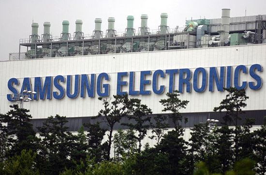
Samsung to invest additional $9.2 billion in its $14.4 billion fab
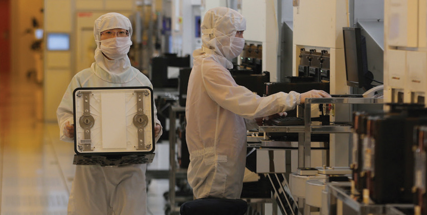
Noticia:Samsung Electronics plans to invest additional $9.2 billion in capacity expansion of the world’s largest semiconductor fab, a media report claims. At present it is unclear how exactly Samsung plans to expand its fab, but the cost of the whole project – around $23.6 billion – already looks staggering.
Samsung announced plans to build its gigantic semiconductor manufacturing facility near Pyeongtaek, South Korea, last October. The fab is expected to be twice as wide as Samsung’s S1 plant in Giheung, South Korea, and can accommodate up to five semiconductor production lines, it was revealed earlier this month. The production facility is expected to be used primarily for DRAM [dynamic random access memory]. The plant requires investment of 15.6 trillion won ($14.4 billion) and is set to begin operations in 2017.
 Samsung S1 fab in Giheung, South Korea. Image by ThanhnienNews
Even though exact production capacity of the fab remains unknown, keeping in mind that it is bigger than Samsung’s S1 semiconductor fabrication plant, which can process 170 thousand of 300mm wafers a month, it is likely that the new fab will be the world’s first plant with capacity of at least 300 thousand 300mm wafer starts per month.
Samsung is not standing still. Reuters news-agency reports that the company is already mulling capacity expansion investment plan for the semiconductor fab. At this time, the company is expected to spend at least another 10 trillion won ($9.2 billion) to boost capacity at its new manufacturing facility. The report does not reveal when the additional investment is set to take place.
At present it is unclear how exactly Samsung plans to increase production capacity of its fab near Pyeongtaek, South Korea, but there are at least three options:
- Increase the amount of production lines by physically expanding the fab.
- Install extreme ultraviolet (EUV) lithography equipment in existing fab. This could improve yield and lower complexity of manufacturing operations, which could ultimately lead to increase of wafer starts per month and production capacity. EUV equipment will be used for DRAM production one or two years after companies start to use it for production of advanced chips like microprocessors, according to ASML. Since EUV is not going to be used until at least 2017, DRAM will be produced using the new lithography tools only in 2019-2020 at the earliest.
- Convert the fab to 450mm wafers and effectively increase its chip output by 2.25 times. While this plan brings the most benefits, 450mm equipment is not going to be ready for mass production for years. Moreover, transition to 450mm equipment is a risky one in general.
http://www.kitguru.net/components/me...4-billion-fab/
-
24-04-15, 17:15 #65Tech Membro

- Registo
- Mar 2013
- Local
- C.Branco
- Posts
- 2,326
- Likes (Dados)
- 0
- Likes (Recebidos)
- 0
- Avaliação
- 0
- Mentioned
- 0 Post(s)
- Tagged
- 0 Thread(s)
 Post Original de Jorge-Vieira

Entretanto em para os lados da Lisa Su em Sunnyvale...


-
29-04-15, 16:13 #66Tech Ubër-Dominus
- Registo
- Nov 2013
- Local
- City 17
- Posts
- 30,121
- Likes (Dados)
- 0
- Likes (Recebidos)
- 2
- Avaliação
- 1 (100%)
- Mentioned
- 0 Post(s)
- Tagged
- 0 Thread(s)
Globalfoundries 14nm process has volume production levels
Noticia: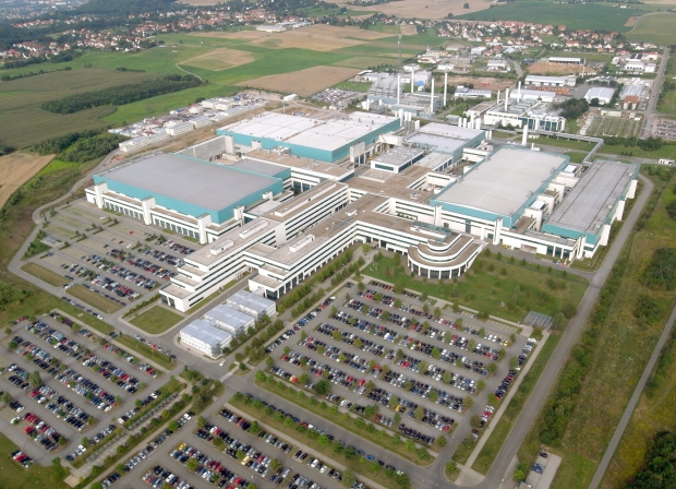
Licenced by Samsung
Globalfoundries is now getting volume production from the 14nm FinFET technology it licensed from Samsung.
According to Expreview the 14nm process consists of LPE (low-power early) and the LPP (Low Power Plus, advanced low power processing) and both are being churned out at the New York, Malta, Fab 8 wafer fab production.
According to the official disclosure of the progress GloFlo's 14nm LPE process has passed certification earlier this year. Now it appears that yields have reached the level of mass production.
The 14nm LPP process is also underway and expected to be certified in the Q3 quarter and get Quarterly volume production in the first quarter of next year.
, GF 14nm LPP also provides additional functionality, such as an additional IP core, 2.5D and 3D TSV packaging, advanced DFM (design for manufacturability) and better EDA reference flow.
The 14nm LPP system is being pushed towards mobile processors and high-performance core product. This includes AMD next-generation CPU and GPU technology which will use 14nm FinFET technology. Since Gloflo is its old chum it is almost certain that AMD will get them first.
Nvidia
Nvidia might use GloFlo tech in its next generation Tegra processor and GPU .This is just a rumour and besides TSMC is its normal partner, but secretly Nvidia might have hooked up with Samsung.
If this is the case then since GloFlo and Samsung are also allies, it is possible that it could get the work.
Nvidia boss Jen-Hsun Huang, admitted that it was possible but refused to confirm or deny if it was happening.
http://www.fudzilla.com/news/process...duction-levels
Boas noticias para a AMD.
-
29-04-15, 16:14 #67Tech Ubër-Dominus
- Registo
- Nov 2013
- Local
- City 17
- Posts
- 30,121
- Likes (Dados)
- 0
- Likes (Recebidos)
- 2
- Avaliação
- 1 (100%)
- Mentioned
- 0 Post(s)
- Tagged
- 0 Thread(s)
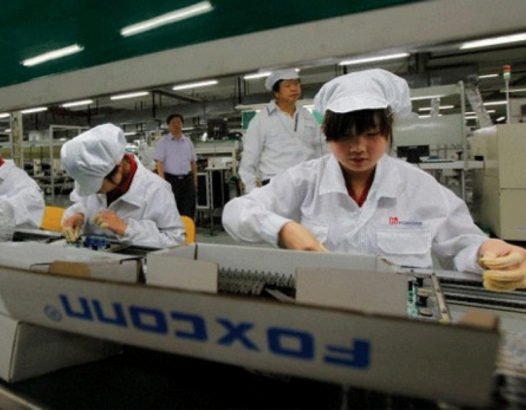
Foxconn steered Apple to TSMC
Noticia: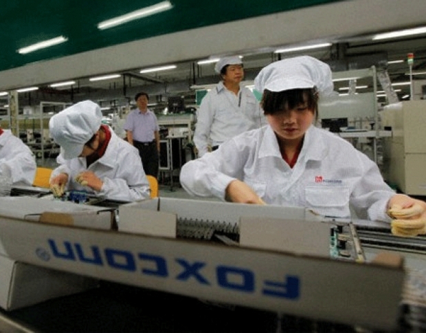
Politics
Foxconn, Apple's main supplier, might have steered Jobs' Mob to TSMC to spite the spite Samsung and keep the money in Taiwan.
The Economic Daily News has suggested that Foxconn CEO Terry Gou talked Apple into awarding some A9 chip orders to TSMC as a way of spiting Samsung for being too successful with its Galaxy S.
Samsung was supposed to make all the next-gen iPhone and iPad processors but at the last minute Apple appeared to change its mind and awarded 30 per cent of the deal to TSMC.
Others claimed that Apple made a decision to purchase A9 chips from TSMC to have enough A9 supply for future devices.
TSMC was lready an Apple partner, as the company has been hired to make the chips in current iPhone and iPad models. Foxconn is the biggest device manufacturer in the world, responsible for mass-producing iPhone 6 models, among other products.
The company has already given Apple preferential treatment when it comes to manufacturing lines, and is said to have invested in a display facility that would operate just to meet Apple's future demands.
Gou's reasoning for supporting TSMC for the next-gen iPhone seems to be a political one, as the executive wants to rally Taiwan-based companies against South Korean companies, especially Samsung.
http://www.fudzilla.com/news/mobile/...-apple-to-tsmc
-
02-05-15, 07:45 #68Tech Ubër-Dominus
- Registo
- Nov 2013
- Local
- City 17
- Posts
- 30,121
- Likes (Dados)
- 0
- Likes (Recebidos)
- 2
- Avaliação
- 1 (100%)
- Mentioned
- 0 Post(s)
- Tagged
- 0 Thread(s)
AMD may be developing APUs for TSMC’s 16nm FinFET process technology
Noticia:Although leaked roadmaps of Advanced Micro Devices indicate that the company’s next year’s accelerated processing units and central processing units will all be made using 14nm FinFET fabrication process at GlobalFoundries, this does not mean that AMD plans to cease using Taiwan Semiconductor Manufacturing Co. as a production partner.
For many years AMD has used both GlobalFoundries and TSMC as its key manufacturing partners. GlobalFoundries focused on higher-end APUs and CPUs, whereas TSMC produced GPUs, inexpensive APUs as well as semi-custom APUs. Last year AMD expanded its orders to GlobalFoundries with select GPUs and semi-custom system-on-chips for game consoles. Next year all key APUs and CPUs from AMD, including “Summit Ridge”, “Bristol Ridge”, “Basilisk” and “Styx” will be made using 14nm FinFET process technology at GlobalFoundries.
Taiwan Semiconductor Manufacturing Co. will likely continue to produce at least some graphics processors for AMD next year. Besides, a quick look at activities of AMD engineers at LinkedIn reveals that many people are (or, perhaps, were) working on accelerated processing units to be made using 16nm FinFET process technology at TSMC. The engineers do not reveal code-names of projects they are (or were) working on.

Many fabless chip designers are not confident of manufacturing capacities and yields of products made using various FinFET manufacturing processes. To mitigate risks associated with yields and production capacities, numerous developers create similar chips for different contract makers of semiconductors so to ensure stable supply.
AMD could take the approach and use TSMC as its second source if it needs. However, given that AMD is cash strapped and does not require extremely high volumes of APUs and CPUs, it is unlikely that the company is re-designing any of its PC chips for TSMC’s process technology. What is possible is that some of the company’s engineers are working on certain semi-custom APUs to be made using 16nm FinFET process technology. Perhaps, Microsoft and Sony would like to get more energy-efficient system-on-chips for Xbox One and PlayStation 4 next year and are willing to pay for appropriate redesigns.
http://www.kitguru.net/components/an...ss-technology/
-
03-05-15, 08:41 #69Tech Ubër-Dominus
- Registo
- Nov 2013
- Local
- City 17
- Posts
- 30,121
- Likes (Dados)
- 0
- Likes (Recebidos)
- 2
- Avaliação
- 1 (100%)
- Mentioned
- 0 Post(s)
- Tagged
- 0 Thread(s)
GlobalFoundries is working on 10nm process technology internally
Noticia:Just like other contract makers of semiconductors, GlobalFoundries is already developing its next-generation 10nm process technology. However, despite of the fact that GlobalFoundries is about to acquire IBM’s semiconductor manufacturing business and the company’s close ties to Samsung Electronics, the 10nm fabrication tech is developed completely internally at the moment.
GlobalFoundries was late with its 28nm process technology and development of its 14nm-XM manufacturing tech took longer than expected. In a bid to offer its customers a leading-edge technology in 2015 – 2016 timeframe, GlobalFoundries licensed Samsung Electronics 14nm LPE [low power early] and LPP [low power plus] processes last year. At present, the company is ramping up production of one 14nm chip and it is expected to hit high volumes later this year.
In October, 2014, IBM announced a definitive agreement to divest its microelectronics business and manufacturing operations to GlobalFoundries. IBM’s semiconductor production unit employs a lot of world-class engineers, who could take part in creation of GF’s 10nm process tech, at least on the late stages. However, at this time 10nm-related research and development activities are conducted completely internally, said Shubhankar Basu, product line manager for leading edge technologies at GlobalFoundries, in an interview with SemiWiki. He did not reveal when did the company start its 10nm development, but it is likely that initial R&D operations began in late 2013 – early 2014.

Since the deal to acquire IBM’s microelectronics business has not yet closed, there are limits, beyond which the companies cannot collaborate. As a result, IBM’s engineers are not currently involved in development of GlobalFoundries 10nm fabrication process.
Modern semiconductor process technologies cost over a billion of dollars to develop and companies tend to use all resources available to make their manufacturing processes better. As a result, it is a pity that GlobalFoundries could not design its 10nm process using IBM’s engineers and intellectual property. Potentially, this means that the company might need to redesign certain parts of the process to add technologies developed by IBM. Alternatively, GlobalFoundries could offer two versions of its 10nm technology to clients: one designed fully in-house and another developed in collaboration with IBM engineers.
http://www.kitguru.net/components/cp...gy-internally/
A GF também não quer ficar para trás nos processos de fabrico
-
05-05-15, 09:03 #70Tech Ubër-Dominus
- Registo
- Nov 2013
- Local
- City 17
- Posts
- 30,121
- Likes (Dados)
- 0
- Likes (Recebidos)
- 2
- Avaliação
- 1 (100%)
- Mentioned
- 0 Post(s)
- Tagged
- 0 Thread(s)
STMicroelectronics will not develop 10nm process technology
Noticia:STMicroelectronics, one of a few semiconductor manufacturers from Europe, said that it would not develop 10nm process technology. Essentially, this means that the company will close its chip manufacturing facility in Crolles, France, at some point in the future.
“We do not have any 10nm planned, and we do not have any activity to invest in 10nm,” said Carlo Bozotti, chief executive officer of STMicroelectronics, during the company’s conference call with investors and financial analysts.
Apparently, 14nm fabrication technology will be the last manufacturing process developed by STMicroelectronics and the company will not produce any chips using 10nm process itself. Going forward the company will likely outsource production of leading edge chips to contract manufacturers. Eventually, its own semiconductor manufacturing facility will be shut down, but that is not going to happen shortly.

STM used to design its process technologies together with NXP, Freescale and Taiwan Semiconductor Manufacturing Co. At some point, its Crolles Alliance was disbanded and STM began to license manufacturing processes from IBM and adapt them at its facility in Crolles, France. Since IBM is about to sell its microelectronics business unit to GlobalFoundries, the company will no longer develop fabrication processes. As a result, STM will be unable to license manufacturing technologies.
ST’s previous CEO Pasquale Pistorio argued that every region of the world needs controlled access to advanced microelectronics, reports Electronics Weekly. Unfortunately, it looks like after 14nm, Europe will not have its own leading-edge manufacturing technology. While GlobalFoundries could upgrade its Fab 1 in Dresden, Germany, its process technologies cannot be called purely European.
http://www.kitguru.net/components/an...ss-technology/
-
29-05-15, 15:58 #71Tech Ubër-Dominus
- Registo
- Nov 2013
- Local
- City 17
- Posts
- 30,121
- Likes (Dados)
- 0
- Likes (Recebidos)
- 2
- Avaliação
- 1 (100%)
- Mentioned
- 0 Post(s)
- Tagged
- 0 Thread(s)
TSMC to move to 16FF+ in next six months
Noticia: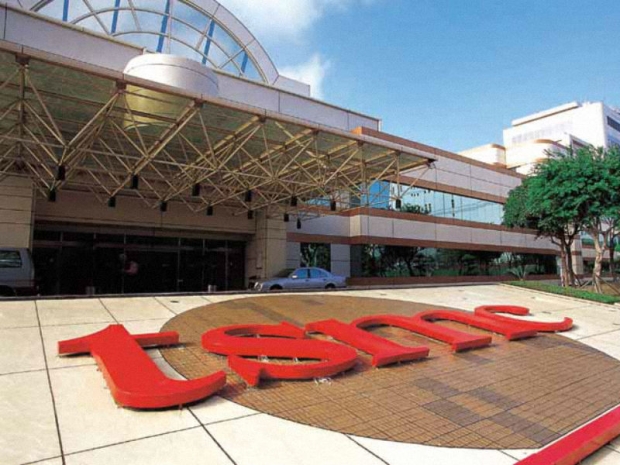
Foundry plans to triple 16nm capacity in 2016
TSMC's 16nm FinFET process has barely gotten off the ground, but the foundry is already talking about 16nm FinFET Plus, which is due to launch by the end of the year.
The improved 16nm FinFET Plus (16FF+) node is supposed to deliver more efficiency and performance, making TSMC's node more competitive compared to Samsung's 14nm node. That is the general idea, but TSMC's first generation 16nm node has failed to impress in terms of design wins. TSMC president CC Wei said the new 16FF+ node already has 20 tapeouts, ten of which achieved satisfactory yield performance. Wei said the company expects up to 50 tapeouts by the end of the year. TSMC expects 16FF+ to enter commercial production in the second half of the year.
16FF+ is not the only FinFET node coming from TSMC over the next year. The company plans to introduce 16FFC for compact devices sometime in the second half of 2016. In addition, 10nm FinFET is expected to enter risk production by the end of 2015, reports Digitimes.
http://www.fudzilla.com/news/process...ext-six-months
-
20-06-15, 14:37 #72Tech Ubër-Dominus
- Registo
- Nov 2013
- Local
- City 17
- Posts
- 30,121
- Likes (Dados)
- 0
- Likes (Recebidos)
- 2
- Avaliação
- 1 (100%)
- Mentioned
- 0 Post(s)
- Tagged
- 0 Thread(s)
Nvidia and Samsung still cannot finalize chip manufacturing deal
Noticia:Earlier this year Nvidia Corp. officially named Samsung Electronics its manufacturing partner. However, as it appears, the companies still have not signed any actual deals because negotiations are proceeding with difficulties. The consequence of prolonged negotiations could result in later-than-expected release of Samsung-made Nvidia chips.
Nvidia wants Samsung Electronics to guarantee certain level of yield rate at 14nm for its graphics processing units, reports BusinessKorea. The yield rate is as a condition of a provisional contract with Samsung Electronics, the web-site emphasizes. The negotiations are proceeding with difficulties because Samsung’s 14nm low-power plus (14LPP) fabrication process is still not really mature.
Theoretically, engineering and business decision operations are isolated. Nvidia’s chip designers are working on chips to be made by Samsung, whereas other people are negotiating over pricing. If talks take too much time, then the start of volume production may be delayed, but since Nvidia will need Samsung’s production services only in 2016, it still has weeks or even months to negotiate a deal.
At present, Samsung Foundry is the only contract maker of semiconductors that produces chips using 14nm FinFET process technology in high volume. Taiwan Semiconductor Manufacturing Co. is expected to start mass production of chips using its 16nm FinFET process this month. Intel Corp.’s foundry division offers 14nm FinFET services to select companies and, based on rumours, not everyone is happy with the technology.
According to unofficial information, Nvidia recently taped out its first code-named GP100 graphics processing unit, which belongs to the “Pascal” family of products. The chip is set to be produced using TSMC’s 16nm FinFET+ (CLN16FF+) fabrication process.

One analyst believes that Nvidia plans to use its contract with Samsung’s not only to get access to leading-edge fabrication processes and to ensure high-volume supply of chips, but also in order to cut-down its costs. In fact, a number of fabless semiconductor designers are believed to be using contracts with Samsung as a leverage in their negotiations with TSMC over pricing.
“We believe that Nvidia has a second source for foundry wafers in Samsung, outside of TSMC,” said Doug Freedman, an analyst with RBC Capital Markets, in a note to clients. “While it may be a small part of the wafer supply today, it should create a tailwind for [gross margin percentage] going forward as we believe that non-TSMC wafers can be purchased at as much as 10% below present cost levels.”
Nvidia and Samsung did not comment on the news-story.
http://www.kitguru.net/components/gr...acturing-deal/
Será que a nvidia vai procurar outro?
E quem será, GF ou novamente a TSMC?
-
24-06-15, 08:50 #73Tech Ubër-Dominus
- Registo
- Nov 2013
- Local
- City 17
- Posts
- 30,121
- Likes (Dados)
- 0
- Likes (Recebidos)
- 2
- Avaliação
- 1 (100%)
- Mentioned
- 0 Post(s)
- Tagged
- 0 Thread(s)
GlobalFoundries is evaluating 22nm FD SOI technology
Noticia:Modern FinFET process technologies help to reduce power consumption of modern chips while increasing their clock-rate potential. Unfortunately, it is extremely expensive to design FinFET chips, which is why many chip developers cannot afford creation of new solutions. In a bid to help such companies to release new chips, GlobalFoundries is evaluating 22nm FD SOI process technology, which will be cheaper than FinFET, but will offer similar performance.
22nm fully-depleted silicon-on-insulator process technology guarantees high clock-rates as well as minimal power consumption in idle mode, something tremendously important for Internet-of-Things and wearable devices. From design cost perspective, 22nm FD-SOI is comparable to 28nm planar technology and is dramatically more affordable than 14nm FinFET process. GlobalFoundries hopes that 22nm FD-SOI provides performance comparable to that of FinFET technologies.
“We are evaluating an advanced node FD-SOI product offering, but we are not ready to disclose detailed plans at this time,” said Jason Gorss, a spokesman for GlobalFoundries. “We believe the right FD-SOI offering can enable significant customer value, especially in small-die, low-cost markets. FDSOI is gaining interest because it can approach FinFET-like performance, it has a cost per die comparable to 28poly/SiON, and it can be optimized with varying levels of performance and leakage to satisfy differentiated customer requirements. It also has low process complexity and significantly fewer mask layers than a FinFET process.”
At present it is unclear when GlobalFoundries will actually make its 22nm FD SOI fabrication process available to customers.
http://www.kitguru.net/components/an...oi-technology/
-
26-06-15, 13:18 #74Tech Ubër-Dominus
- Registo
- Nov 2013
- Local
- City 17
- Posts
- 30,121
- Likes (Dados)
- 0
- Likes (Recebidos)
- 2
- Avaliação
- 1 (100%)
- Mentioned
- 0 Post(s)
- Tagged
- 0 Thread(s)
More details about GlobalFoundries’ 22nm FD-SOI emerge
Noticia:GlobalFoundries has revealed additional details regarding its 22nm fully-depleted silicon-on-insulator (FD-SOI) fabrication technology. The manufacturing process will be ready for tape-outs in early 2016 and will be used for mass production of chips by late next year. While the tech has a number of advantages, the process is designed primarily for small high-volume chips and designers of larger ICs will hardly be interested in using it.
“We are developing 22nm FD-SOI process technology right now,” said Gerd Teepe, director and design engineering at GlobalFoundries, reports EETimes. “The plan is to qualify the process by early 2016 and start volume production by the end of 2016.”
GlobalFoundries 22nm FD-SOI will use back-end-of-line (BEOL) interconnect flow of STMicroelectronics’ 28nm FD-SOI as well as front-end of line (FEOL) of STM’s 14nm FD-SOI. Just like two aforementioned process technologies from STM, GlobalFoundries’ 22nm FD-SOI is a planar technology with fewer metal layers and mask steps compared to fabrication processes, which use FinFET transistors. However, unlike STM’s 14nm FD-SOI, the new tech from GlobalFoundries does not require double-patterning anywhere, which simplifies chip design.
“We are using STMicroelectronics’ 14nm FD-SOI in our frontend, while using 28nm FD-SOI in the backend,” explained Mr. Teepe.
Since the 22nm FD-SOI relies on a 28nm BEOL, die sizes of chips produced using the technology will be similar to those made using 28nm nodes. As a result, it will not make a lot of sense for makers of large chips to transit to 22nm FD-SOI since they will increase their costs (FD-SOI wafers are more expensive than bulk wafers), but will not be able to introduce a lot of new features without considerably increasing their die sizes (which increases costs further). For makers of smaller high-volume ICs [integrated circuits] it makes considerably more sense to adopt 22nm FD-SOI since they keep their design costs and power consumption low, but will be able to increase performance.
Initially, GlobalFoundries will address its existing SOI customers with the technology, but eventually the tech and its successors will be offered to designers of chips for wearable and Internet-of-Things devices.
“We hope to be able to leverage FD-SOI’s super low-power strategy for wearables and other products, whose volume will start to emerge by then,” said Mr. Teepe.
GlobalFoundries’ 22nm FD-SOI is compatible with neither 14nm nor 28nm FD-SOI, hence, customers to STMicroelectronics and Samsung Foundry (which licenses 28nm FD-SOI from STM) will have to re-implement their chips for the new process.
http://www.kitguru.net/components/an...fd-soi-emerge/
-
01-07-15, 13:50 #75Tech Ubër-Dominus
- Registo
- Nov 2013
- Local
- City 17
- Posts
- 30,121
- Likes (Dados)
- 0
- Likes (Recebidos)
- 2
- Avaliação
- 1 (100%)
- Mentioned
- 0 Post(s)
- Tagged
- 0 Thread(s)
U.S. clears acquisition of IBM’s chip unit by GlobalFoundries
Noticia:GlobalFoundries this week said that the U.S. authorities had approved its acquisition of IBM’s microelectronics business unit. From now on, GlobalFoundries will make various important semiconductors for the U.S. military and government agencies.
The Committee on Foreign Investment in the United States (CFIUS) has reviewed the proposed transaction between IBM and GlobalFoundries and concluded in favour of the deal, which means that nothing stops GlobalFoundries from taking over microelectronics operations from IBM. The transaction is expected to close in the near future.
Under the terms of the agreement between IBM and GlobalFoundries, the former will get and operate existing IBM fabs in East Fishkill, New York, and Essex Junction, Vermont. IBM will pay GlobalFoundries $1.5 billion over the next three years in order to take the fabs and respect existing contracts. GlobalFoundries will also get intellectual property, world-class semiconductor specialists and technologies related to IBM Microelectronics. In addition, GlobalFoundries will become IBM’s exclusive server processor maker for 22nm, 14nm and 10nm chips for the next 10 years.

The 200mm fab in Essex Junction, Vermont, produces certain high-end radar and other components for the U.S. government using SiGe and SOI processes, according to a media reports. Typically, the U.S. authorities demand that fabs producing such chips belong to the U.S. companies, but it appears that the CFIUS did not block the transaction.
“This acquisition solidifies GlobalFoundries’ leadership position in semiconductor technology development and manufacturing,” said Sanjay Jha, CEO of GlobalFoundries. “We can now offer our customers a broader range of differentiated leading-edge 3D transistor and RF technologies, and we will also improve our design ecosystem to accelerate time-to-revenue for our customers. This acquisition further strengthens advanced manufacturing in the United States, and builds on established relationships in New York and Vermont.”
IBM needed to get rid of its microelectronics business because the latter had generated a lot of losses for the company.
http://www.kitguru.net/components/an...obalfoundries/


 Responder com Citação


Informação da Thread
Users Browsing this Thread
Estão neste momento 1 users a ver esta thread. (0 membros e 1 visitantes)
 Regras
São agora 22:58.
 User Alert System provided by
Advanced User Tagging v3.3.0 (Lite) -
vBulletin Mods & Addons Copyright © 2024 DragonByte Technologies Ltd.
User Alert System provided by
Advanced User Tagging v3.3.0 (Lite) -
vBulletin Mods & Addons Copyright © 2024 DragonByte Technologies Ltd.
Feedback Buttons provided by Advanced Post Thanks / Like (Lite) - vBulletin Mods & Addons Copyright © 2024 DragonByte Technologies Ltd.
Portugal-Tech 2012-24 | Todos os direitos reservados! Alojamento Powered by: Trignosfera
Powered by vBulletin® Version 4.2.5 Alpha 3
Copyright © 2024 vBulletin Solutions, Inc. All rights reserved.
Copyright © 2024 vBulletin Solutions, Inc. All rights reserved.
Feedback Buttons provided by Advanced Post Thanks / Like (Lite) - vBulletin Mods & Addons Copyright © 2024 DragonByte Technologies Ltd.
Portugal-Tech 2012-24 | Todos os direitos reservados! Alojamento Powered by: Trignosfera
Bookmarks