

Apple Aims to Sell Macs With Its Own Chips Starting in 2021The Cupertino, California-based technology giant is working on three of its own Mac processors, known as systems-on-a-chip, based on the A14 processor in the next iPhone. The first of these will be much faster than the processors in the iPhone and iPad, the people said.
Apple is preparing to release at least one Mac with its own chip next year, according to the people. But the initiative to develop multiple chips, codenamed Kalamata, suggests the company will transition more of its Mac lineup away from current supplier Intel Corp.
Taiwan Semiconductor Manufacturing Co., Apples partner for iPhone and iPad processors, will build the new Mac chips, said the people, who asked not to be identified discussing private product plans. The components will be based on a 5-nanometer production technique, the same size Apple will use in the next iPhones and iPad Pros, one of the people said. An Apple spokesman declined to comment, as did Intel and TSMC.
This news has negative longer-term implications for Intel, in-line with our concerns around Intels future market share, Brad Gastwirth, chief technology strategist at Wedbush Securities, wrote in a note to investors. Shares of the chipmaker fell as much as 2.2% on Thursday while the rest of the market rose.
The Kalamata project has been going for several years. In 2018, Apple developed a Mac chip based on the iPad Pros A12X processor for internal testing. That gave the companys engineers confidence they could begin replacing Intel in Macs as early as 2020, Bloomberg News reported.
E com este golpe, o mercado X86 fica um bocado mais pequeno.

User Tag List
 Likes: 0
Resultados 1 a 14 de 14
Tópico: Apple CPU "Kalamata"
-
29-04-20, 22:45 #1Moderador


- Registo
- Feb 2013
- Local
- Santo Tirso
- Posts
- 12,672
- Likes (Dados)
- 30
- Likes (Recebidos)
- 208
- Avaliação
- 4 (100%)
- Mentioned
- 7 Post(s)
- Tagged
- 0 Thread(s)
Apple CPU "Kalamata"
Ryzen R5 3700X / Noctua NH-D15 / B550 AORUS ELITE V2 / Cooler Master H500 Mesh / 16Gb DDR4 @ 3800mhz CL16 / Gigabyte RTX 2070 Super / Seasonic Focus GX 750W / Sabrent Q Rocket 2 TB / Crucial MX300 500Gb + Samsung 250Evo 500Gb / Edifier R1700BT
-
30-04-20, 01:20 #2Tech Membro

- Registo
- Aug 2014
- Posts
- 1,136
- Likes (Dados)
- 14
- Likes (Recebidos)
- 10
- Avaliação
- 0
- Mentioned
- 0 Post(s)
- Tagged
- 0 Thread(s)
Tempos negros para a intel.
Laptops: amd
Desktops: amd
Servers: amd
Consoles: amd
Mobile: Qualcomm
Restam chips de networking e pouco mais.
Com a estagnação da Intel e falhas na segurança está visto que vão fazer tudo e mandá-los á fava.
Assim também controlam todo o processo. Evitam também a tentação da malta usar Windows nos macs.
-
09-06-20, 13:38 #3Moderador
- Registo
- Feb 2013
- Local
- Santo Tirso
- Posts
- 12,672
- Likes (Dados)
- 30
- Likes (Recebidos)
- 208
- Avaliação
- 4 (100%)
- Mentioned
- 7 Post(s)
- Tagged
- 0 Thread(s)
Apple Plans to Announce Move to Its Own Mac Chips at WWDC
Estão quase a chegar. Será que é desta que vemos os X86 a perder a coroa de CPUs mais rápidos do mundo?Apple Inc. is preparing to announce a shift to its own main processors in Mac computers, replacing chips from Intel Corp., as early as this month at its annual developer conference, according to people familiar with the plans.The company is holding WWDC the week of June 22. Unveiling the initiative, codenamed Kalamata, at the event would give outside developers time to adjust before new Macs roll out in 2021, the people said. Since the hardware transition is still months away, the timing of the announcement could change, they added, while asking not to be identified discussing private plans.
The new processors will be based on the same technology used in Apple-designed iPhone and iPad chips. However, future Macs will still run the macOS operating system rather than the iOS software on mobile devices from the company. Bloomberg News reported on Apple’s effort to move away from Intel earlier this year, and in 2018.
Apple is using technology licensed from Arm Ltd., part of Japanese tech conglomerate SoftBank Group Corp. This architecture is different from the underlying technology in Intel chips, so developers will need time to optimize their software for the new components. Cupertino, California-based Apple and Santa Clara-based Intel declined to comment.
This will be the first time in the 36-year history of the Mac that Apple-designed processors will power these machines. It has changed chips only two other times. In the early 1990s, Apple switched from Motorola processors to PowerPC. At WWDC in 2005, Steve Jobs announced a move from PowerPC to Intel, and Apple rolled out those first Intel-based Macs in January 2006. Like it did then, the company plans to eventually transition the entire Mac lineup to its Arm-based processors, including the priciest desktop computers, the people said.
Read more: Apple Aims to Sell Macs With Its Own Chips Starting in 2021
Apple has about 10% of the PC market, so the change may not cut into Intel sales much. However, Macs are considered premium products. So if the company moves away from Intel for performance reasons it may prompt other PC makers to look at different options, too. Microsoft Corp., Samsung Electronics Co. and Lenovo Group Ltd. have already debuted laptops that run on Arm-based chips.
Apple’s chip-development group, led by Johny Srouji, decided to make the switch after Intel’s annual chip performance gains slowed. Apple engineers worried that sticking to Intel’s road map would delay or derail some future Macs, according to people familiar with the effort.
Inside Apple, tests of new Macs with the Arm-based chips have shown sizable improvements over Intel-powered versions, specifically in graphics performance and apps using artificial intelligence, the people said. Apple’s processors are also more power-efficient than Intel’s, which may mean thinner and lighter Mac laptops in the future.
Apple’s move would be a highlight of this year’s WWDC, which will be held online due to the Covid-19 pandemic. Because of the fluid nature of the global health crisis and its impact on Apple’s product development, the timing of the chip announcement could change.
At the conference, Apple is also readying updates to its other operating systems -- iOS, iPadOS, tvOS and watchOS -- with changes to augmented-reality capabilities, deeper integration with outside apps and services, and improved Apple Watch fitness features. A big priority is improving the performance of its mobile software after last year’s release, iOS 13, suffered from several issues.
The company is working on at least three of its own Mac processors, known as systems-on-a-chip, with the first based on the A14 processor in the next iPhone. In addition to the main central processing unit, there will be a graphics processing unit and a Neural Engine for handling machine learning, a popular and powerful type of AI, the people said. In the past, Apple has made chips for specific Mac functions, such as security.
Read more about Apple’s upcoming Mac chips here.
Intel has faced more competition as its lead in production technology -- a key way to improve semiconductor performance -- has slipped. Taiwan Semiconductor Manufacturing Co. makes processors for many of Intel’s rivals using a more advanced process.
TSMC will build the new Mac processors using a 5-nanometer production technique -- the same approach as for the next iPhones and iPad Pros. Intel rivals Qualcomm Inc. and Advanced Micro Devices Inc. also use TSMC to make their chips.
Ryzen R5 3700X / Noctua NH-D15 / B550 AORUS ELITE V2 / Cooler Master H500 Mesh / 16Gb DDR4 @ 3800mhz CL16 / Gigabyte RTX 2070 Super / Seasonic Focus GX 750W / Sabrent Q Rocket 2 TB / Crucial MX300 500Gb + Samsung 250Evo 500Gb / Edifier R1700BT
-
09-06-20, 14:37 #4Tech Membro
- Registo
- Aug 2014
- Posts
- 1,136
- Likes (Dados)
- 14
- Likes (Recebidos)
- 10
- Avaliação
- 0
- Mentioned
- 0 Post(s)
- Tagged
- 0 Thread(s)
Aquela malta dos kac pro devem estar a ver o dinheiro ir ao ar. Ainda que mantenham o suporte para Intel. Por quanto tempo?
-
09-06-20, 14:57 #5O Administrador

- Registo
- Mar 2013
- Local
- Multiverso
- Posts
- 17,814
- Likes (Dados)
- 74
- Likes (Recebidos)
- 156
- Avaliação
- 31 (100%)
- Mentioned
- 31 Post(s)
- Tagged
- 0 Thread(s)
Boas!
Questões meramente $$$$ ... Cortar o middle man... e ir para ARM com a ajuda de algum fabricante chinoca...
Aqui o problema é que o ARM nas suas revisões mais recentes tem ganho em termos de performance para começar a ser relevante...
A não ser que o X86 dê algum salto, na próxima década deve começar a cair na decadência...
Cumprimentos,
LPCMy Specs: .....
CPU: AMD Ryzen 7 5800X3D :-: Board: MSI B550M BAZOOKA :-: RAM: 64 GB DDR4 Kingston Fury Renegade 3600 Mhz CL16 :-: Storage: Kingston NV2 NVMe 2 TB + Kingston NV2 NVMe 1 TB
CPU Cooling Solution: ThermalRight Frost Commander 140 Black + ThermalRight TL-C12B-S 12CM PWM + ThermalRight TL-C14C-S 14CM PWM :-: PSU: Corsair HX 1200 WATTS
Case: NZXT H6 FLOW :-: Internal Cooling: 4x ThermalRight TL-C12B-S 12CM PWM + 4x ThermalRight TL-C14C-S 14CM PWM
GPU: ASUS TUF AMD RADEON RX 7900 XTX - 24 GB :-: Monitor: BenQ EW3270U 4K HDR
-
23-06-20, 09:40 #6Moderador
- Registo
- Feb 2013
- Local
- Santo Tirso
- Posts
- 12,672
- Likes (Dados)
- 30
- Likes (Recebidos)
- 208
- Avaliação
- 4 (100%)
- Mentioned
- 7 Post(s)
- Tagged
- 0 Thread(s)
E começou a transição de X86 para ARM, para a Apple.
E o mesmo deve acontecer com os GPUs da AMD.
The Next Phase: Apple Lays Out Plans To Transition Macs from x86 to Apple SoCs
Ryzen R5 3700X / Noctua NH-D15 / B550 AORUS ELITE V2 / Cooler Master H500 Mesh / 16Gb DDR4 @ 3800mhz CL16 / Gigabyte RTX 2070 Super / Seasonic Focus GX 750W / Sabrent Q Rocket 2 TB / Crucial MX300 500Gb + Samsung 250Evo 500Gb / Edifier R1700BT
-
25-06-20, 12:49 #7Moderador
- Registo
- Feb 2013
- Local
- Santo Tirso
- Posts
- 12,672
- Likes (Dados)
- 30
- Likes (Recebidos)
- 208
- Avaliação
- 4 (100%)
- Mentioned
- 7 Post(s)
- Tagged
- 0 Thread(s)
Bad Intel Quality Assurance Responsible for Apple-Intel Split?
Apple's decision to switch from Intel processors for its Mac computers to its own, based on the Arm architecture, has shaken up the tech world, even though rumors of the transition have been doing rounds for months. Intel's first official response, coupled with facts such as Intel's CPU technology execution being thrown completely off gear due to foundry problems; pointed toward the likelihood of Intel not being able to keep up with Apple's growing performance/Watt demands. It turns out now, that Intel's reasons are a lot more basic, and date back to 2016.
According to a sensational PC Gamer report citing former Intel principal engineer François Piednoël, Apple's dissatisfaction with Intel dates back to some of its first 14 nm chips, based on the "Skylake" microarchitecture. "The quality assurance of Skylake was more than a problem," says Piednoël. It was abnormally bad. We were getting way too much citing for little things inside Skylake. Basically our buddies at Apple became the number one filer of problems in the architecture. And that went really, really bad. When your customer starts finding almost as much bugs as you found yourself, you're not leading into the right place," he adds.
It was around that time that decisions were taken at the highest levels in Apple to execute a machine architecture switch away from Intel and x86, the second of its kind following Apple's mid-2000s switch from PowerPC to Intel x86. For me this is the inflection point," says Piednoël. "This is where the Apple guys who were always contemplating to switch, they went and looked at it and said: 'Well, we've probably got to do it.' Basically the bad quality assurance of Skylake is responsible for them to actually go away from the platform." Apple's decision to dump Intel may have only been more precipitated with 2019 marking a string of cybersecurity flaws affecting Intel microarchitectures. The PC Gamer report cautions that Piednoël's comments should be taken with a pinch of salt, as he has been among the more outspoken engineers at Intel.Ryzen R5 3700X / Noctua NH-D15 / B550 AORUS ELITE V2 / Cooler Master H500 Mesh / 16Gb DDR4 @ 3800mhz CL16 / Gigabyte RTX 2070 Super / Seasonic Focus GX 750W / Sabrent Q Rocket 2 TB / Crucial MX300 500Gb + Samsung 250Evo 500Gb / Edifier R1700BT
-
11-11-20, 18:51 #8Moderador
- Registo
- Feb 2013
- Local
- Santo Tirso
- Posts
- 12,672
- Likes (Dados)
- 30
- Likes (Recebidos)
- 208
- Avaliação
- 4 (100%)
- Mentioned
- 7 Post(s)
- Tagged
- 0 Thread(s)
A Apple apresentou o seu A14 para laptos e desktops e é uma besta.
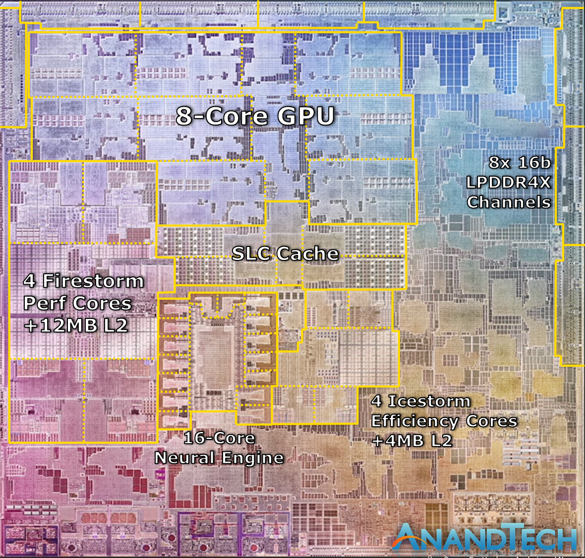
Apple Announces The Apple Silicon M1: Ditching x86 - What to Expect, Based on A14The new Apple M1 is really the start of a new major journey for Apple. During Apple’s presentation the company didn’t really divulge much in the way of details for the design, however there was one slide that told us a lot about the chip’s packaging and architecture:
This packaging style with DRAM embedded within the organic packaging isn't new for Apple; they've been using it since the A12. However it's something that's only sparingly used. When it comes to higher-end chips, Apple likes to use this kind of packaging instead of your usual smartphone POP (package on package) because these chips are designed with higher TDPs in mind. So keeping the DRAM off to the side of the compute die rather than on top of it helps to ensure that these chips can still be efficiently cooled.
What this also means is that we’re almost certainly looking at a 128-bit DRAM bus on the new chip, much like that of previous generation A-X chips.
On the very same slide, Apple also seems to have used an actual die shot of the new M1 chip. It perfectly matches Apple’s described characteristics of the chip, and it looks looks like a real photograph of the die. Cue what's probably the quickest die annotation I’ve ever made:
We can see the M1’s four Firestorm high-performance CPU cores on the left side. Notice the large amount of cache – the 12MB cache was one of the surprise reveals of the event, as the A14 still only featured 8MB of L2 cache. The new cache here looks to be portioned into 3 larger blocks, which makes sense given Apple’s transition from 8MB to 12MB for this new configuration, it is after all now being used by 4 cores instead of 2.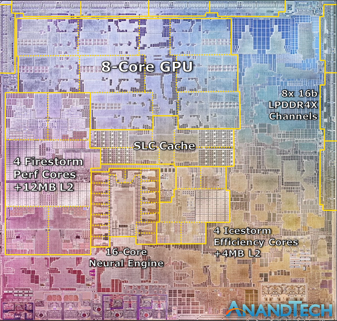
Meanwhile the 4 Icestorm efficiency cores are found near the center of the SoC, above which we find the SoC’s system level cache, which is shared across all IP blocks.
Finally, the 8-core GPU takes up a significant amount of die space and is found in the upper part of this die shot.
What’s most interesting about the M1 here is how it compares to other CPU designs by Intel and AMD. All the aforementioned blocks still only cover up part of the whole die, with a significant amount of auxiliary IP. Apple made mention that the M1 is a true SoC, including the functionality of what previously was several discrete chips inside of Mac laptops, such as I/O controllers and Apple's SSD and security controllers.
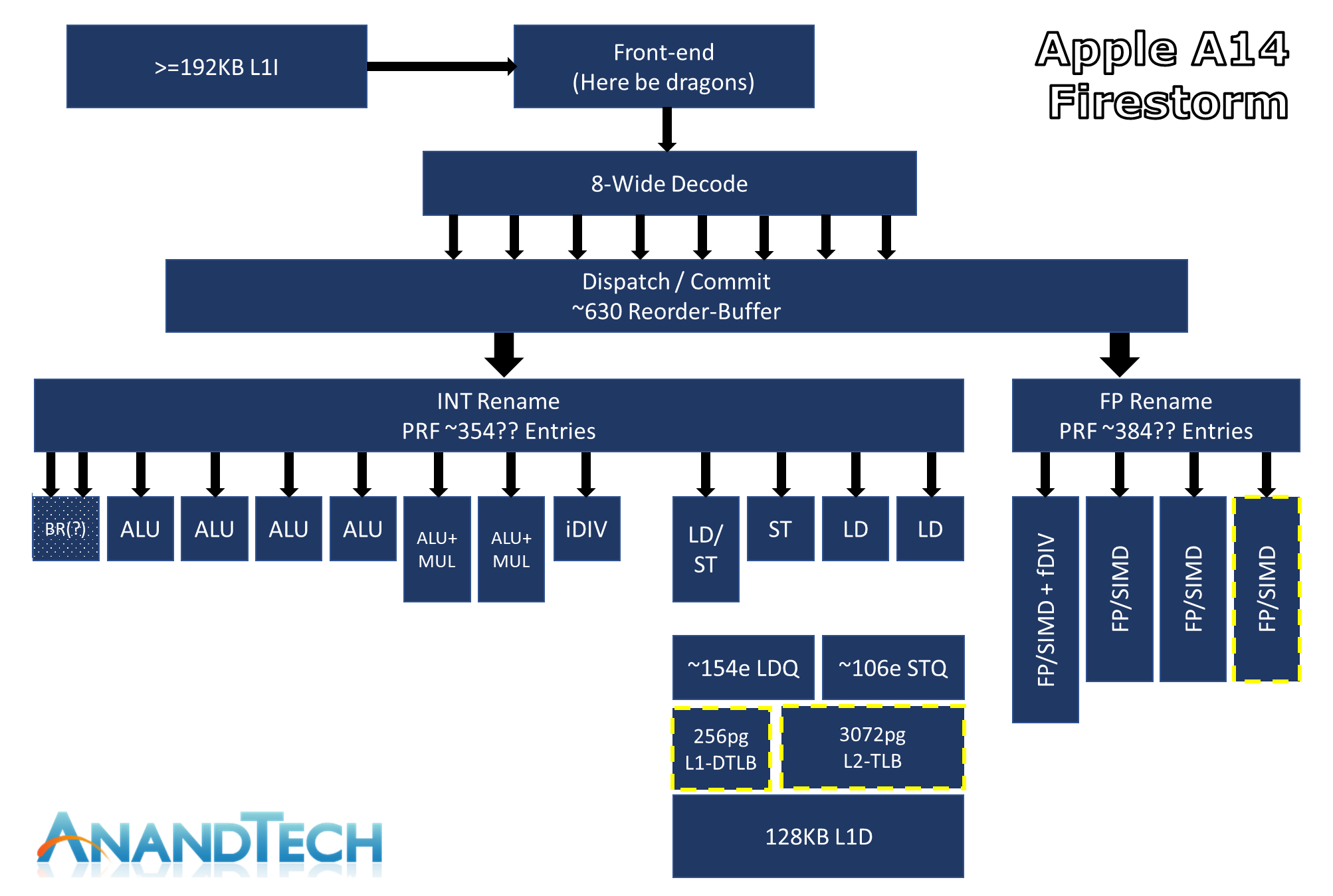
Apple's Firestorm CPU Core: Even Bigger & Wider
Apple’s latest generation big core CPU design inside of the A14 is codenamed “Firestorm”, following up last year’s “Lightning” microarchitecture inside of the Apple A13. The new Firestorm core and its years long pedigree from continued generational improvements lies at the heart of today’s discussion, and is the key part as to how Apple is making the large jump away from Intel x86 designs to their own in-house SoCs.
The above diagram is an estimated feature layout of Apple’s latest big core design – what’s represented here is my best effort attempt in identifying the new designs’ capabilities, but certainly is not an exhaustive drill-down into everything that Apple’s design has to offer – so naturally some inaccuracies might be present.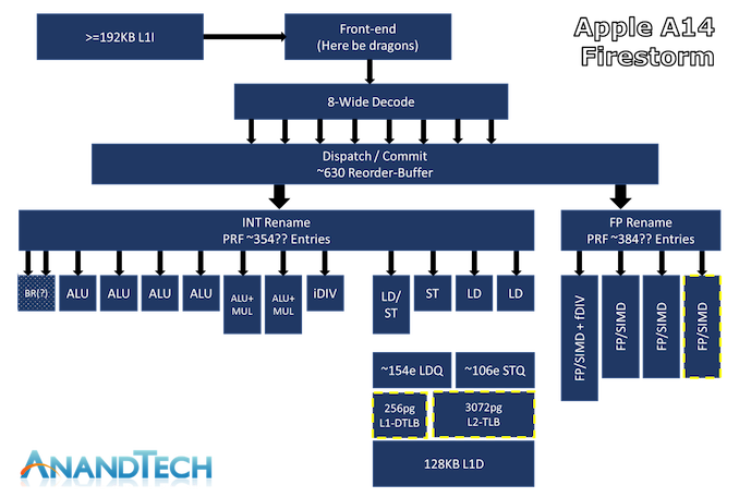
What really defines Apple’s Firestorm CPU core from other designs in the industry is just the sheer width of the microarchitecture. Featuring an 8-wide decode block, Apple’s Firestorm is by far the current widest commercialized design in the industry. IBM’s upcoming P10 Core in the POWER10 is the only other official design that’s expected to come to market with such a wide decoder design, following Samsung’s cancellation of their own M6 core which also was described as being design with such a wide design.
Other contemporary designs such as AMD’s Zen(1 through 3) and Intel’s µarch’s, x86 CPUs today still only feature a 4-wide decoder designs that is seemingly limited from going wider at this point in time due to the ISA’s inherent variable instruction length nature, making designing decoders that are able to deal with aspect of the architecture more difficult compared to the ARM ISA’s fixed-length instructions. On the ARM side of things, Samsung’s designs had been 6-wide from the M3 onwards, whilst Arm’s own Cortex cores had been steadily going wider with each generation, currently 4-wide in currently available silicon, and expected to see an increase to a 5-wide design in upcoming Cortex-X1 cores.
Apple’s microarchitecture being 8-wide actually isn’t new to the new A14. I had gone back to the A13 and it seems I had made a mistake in the tests as I had originally deemed it a 7-wide machine. Re-testing it recently, I confirmed that it was in that generation that Apple had upgraded from a 7-wide decode which had been present in the A11 and 12.
One aspect of recent Apple designs which we were never really able to answer concretely is how deep their out-of-order execution capabilities are. The last official resource we had on the matter was a 192 figure for the ROB (Re-order Buffer) inside of the 2013 Cyclone design. Thanks again to Veedrac’s implementation of a test that appears to expose this part of the µarch, we can seemingly confirm that Firestorm’s ROB is in the 630 instruction range deep, which had been an upgrade from last year’s A13 Lightning core which is measured in at 560 instructions. It’s not clear as to whether this is actually a traditional ROB as in other architectures, but the test at least exposes microarchitectural limitations which are tied to the ROB and behaves and exposes correct figures on other designs in the industry. An out-of-order window is the amount of instructions that a core can have “parked”, waiting for execution in, well, out of order sequence, whilst the core is trying to fetch and execute the dependencies of each instruction.
A +-630 deep ROB is an immensely huge out-of-order window for Apple’s new core, as it vastly outclasses any other design in the industry. Intel’s Sunny Cove and Willow Cove cores are the second-most “deep” OOO designs out there with a 352 ROB structure, while AMD’s newest Zen3 core makes due with 256 entries, and recent Arm designs such as the Cortex-X1 feature a 224 structure.
Exactly how and why Apple is able to achieve such a grossly disproportionate design compared to all other designers in the industry isn’t exactly clear, but it appears to be a key characteristic of Apple’s design philosophy and method to achieve high ILP (Instruction level-parallelism).
Many, Many Execution Units
Having high ILP also means that these instructions need to be executed in parallel by the machine, and here we also see Apple’s back-end execution engines feature extremely wide capabilities. On the Integer side, whose in-flight instructions and renaming physical register file capacity we estimate at around 354 entries, we find at least 7 execution ports for actual arithmetic operations. These include 4 simple ALUs capable of ADD instructions, 2 complex units which feature also MUL (multiply) capabilities, and what appears to be a dedicated integer division unit. The core is able to handle 2 branches per cycle, which I think is enabled by also one or two dedicated branch forwarding ports, but I wasn’t able to 100% confirm the layout of the design here.
The Firestorm core here doesn’t appear to have major changes on the Integer side of the design, as the only noteworthy change was an apparent slight increase (yes) in the integer division latency of that unit.
On the floating point and vector execution side of things, the new Firestorm cores are actually more impressive as they a 33% increase in capabilities, enabled by Apple’s addition of a fourth execution pipeline. The FP rename registers here seem to land at 384 entries, which is again comparatively massive. The four 128-bit NEON pipelines thus on paper match the current throughput capabilities of desktop cores from AMD and Intel, albeit with smaller vectors. Floating-point operations throughput here is 1:1 with the pipeline count, meaning Firestorm can do 4 FADDs and 4 FMULs per cycle with respectively 3 and 4 cycles latency. That’s quadruple the per-cycle throughput of Intel CPUs and previous AMD CPUs, and still double that of the recent Zen3, of course, still running at lower frequency. This might be one reason why Apples does so well in browser benchmarks (JavaScript numbers are floating-point doubles).
Vector abilities of the 4 pipelines seem to be identical, with the only instructions that see lower throughput being FP divisions, reciprocals and square-root operations that only have an throughput of 1, on one of the four pipes.
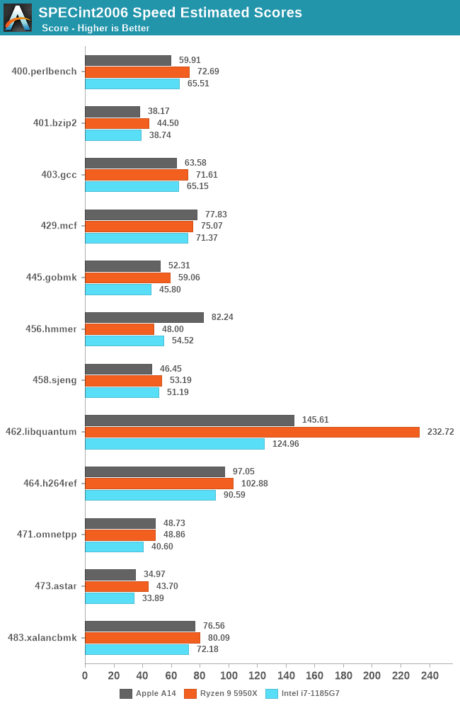
We currently do not have Apple Silicon devices and likely won’t get our hands on them for another few weeks, but we do have the A14, and expect the new Mac chips to be strongly based on the microarchitecture we’re seeing employed in the iPhone designs. Of course, we’re still comparing a phone chip versus a high-end laptop and even a high-end desktop chip, but given the performance numbers, that’s also exactly the point we’re trying to make here, setting the stage as the bare minimum of what Apple could achieve with their new Apple Silicon Mac chips.
Ryzen R5 3700X / Noctua NH-D15 / B550 AORUS ELITE V2 / Cooler Master H500 Mesh / 16Gb DDR4 @ 3800mhz CL16 / Gigabyte RTX 2070 Super / Seasonic Focus GX 750W / Sabrent Q Rocket 2 TB / Crucial MX300 500Gb + Samsung 250Evo 500Gb / Edifier R1700BT
-
13-11-20, 02:03 #9O Administrador
- Registo
- Mar 2013
- Local
- Multiverso
- Posts
- 17,814
- Likes (Dados)
- 74
- Likes (Recebidos)
- 156
- Avaliação
- 31 (100%)
- Mentioned
- 31 Post(s)
- Tagged
- 0 Thread(s)
Boas!
Excelente CPU e super competitivo com o mercado restante...
Se ligarmos isto ao OS fechado e optimizado para aqueles recursos específicos, temos aqui um belo ecosistema.
Cumprimentos,
LPCMy Specs: .....
CPU: AMD Ryzen 7 5800X3D :-: Board: MSI B550M BAZOOKA :-: RAM: 64 GB DDR4 Kingston Fury Renegade 3600 Mhz CL16 :-: Storage: Kingston NV2 NVMe 2 TB + Kingston NV2 NVMe 1 TB
CPU Cooling Solution: ThermalRight Frost Commander 140 Black + ThermalRight TL-C12B-S 12CM PWM + ThermalRight TL-C14C-S 14CM PWM :-: PSU: Corsair HX 1200 WATTS
Case: NZXT H6 FLOW :-: Internal Cooling: 4x ThermalRight TL-C12B-S 12CM PWM + 4x ThermalRight TL-C14C-S 14CM PWM
GPU: ASUS TUF AMD RADEON RX 7900 XTX - 24 GB :-: Monitor: BenQ EW3270U 4K HDR
-
13-11-20, 11:05 #10Moderador
- Registo
- Feb 2013
- Local
- Santo Tirso
- Posts
- 12,672
- Likes (Dados)
- 30
- Likes (Recebidos)
- 208
- Avaliação
- 4 (100%)
- Mentioned
- 7 Post(s)
- Tagged
- 0 Thread(s)
Isso é que transforma este CPU numa miséria. Post Original de LPC

O ecossistema da Apple é super restritivo, o que significa que é praticamente inútil para entusiastas.
Junta a isso o preço ridiculamente alto e temos os priores produtos do mercado.Ryzen R5 3700X / Noctua NH-D15 / B550 AORUS ELITE V2 / Cooler Master H500 Mesh / 16Gb DDR4 @ 3800mhz CL16 / Gigabyte RTX 2070 Super / Seasonic Focus GX 750W / Sabrent Q Rocket 2 TB / Crucial MX300 500Gb + Samsung 250Evo 500Gb / Edifier R1700BT
-
13-11-20, 13:53 #11O Administrador
- Registo
- Mar 2013
- Local
- Multiverso
- Posts
- 17,814
- Likes (Dados)
- 74
- Likes (Recebidos)
- 156
- Avaliação
- 31 (100%)
- Mentioned
- 31 Post(s)
- Tagged
- 0 Thread(s)
Boas! Post Original de Winjer
O sistema é preparado para trabalho essencialmente...
Quem quiser jogar ou fazer outra coisa qualquer, não serve...
Não sou fan da Apple nem sequer dos seus produtos, mas sei ver para o que é que servem...
Cumprimentos,
LPCMy Specs: .....
CPU: AMD Ryzen 7 5800X3D :-: Board: MSI B550M BAZOOKA :-: RAM: 64 GB DDR4 Kingston Fury Renegade 3600 Mhz CL16 :-: Storage: Kingston NV2 NVMe 2 TB + Kingston NV2 NVMe 1 TB
CPU Cooling Solution: ThermalRight Frost Commander 140 Black + ThermalRight TL-C12B-S 12CM PWM + ThermalRight TL-C14C-S 14CM PWM :-: PSU: Corsair HX 1200 WATTS
Case: NZXT H6 FLOW :-: Internal Cooling: 4x ThermalRight TL-C12B-S 12CM PWM + 4x ThermalRight TL-C14C-S 14CM PWM
GPU: ASUS TUF AMD RADEON RX 7900 XTX - 24 GB :-: Monitor: BenQ EW3270U 4K HDR
-
13-11-20, 20:51 #12Tech Novato

- Registo
- Mar 2017
- Posts
- 304
- Likes (Dados)
- 0
- Likes (Recebidos)
- 9
- Avaliação
- 2 (100%)
- Mentioned
- 0 Post(s)
- Tagged
- 0 Thread(s)
ARM nunca foi para entusiastas e também não será agora, muito menos quando se trata da Apple.
A eficiência é algo de outro mundo e isso é inegável.
-
17-11-20, 16:52 #13Moderador
- Registo
- Feb 2013
- Local
- Santo Tirso
- Posts
- 12,672
- Likes (Dados)
- 30
- Likes (Recebidos)
- 208
- Avaliação
- 4 (100%)
- Mentioned
- 7 Post(s)
- Tagged
- 0 Thread(s)
Anandtech - The 2020 Mac Mini Unleashed: Putting Apple Silicon M1 To The Test
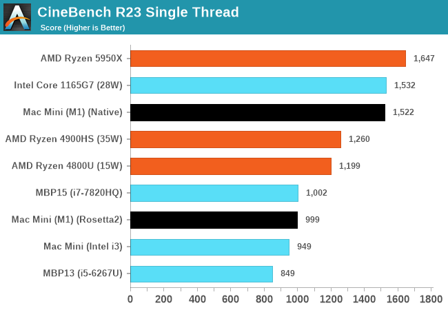
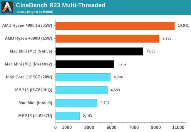
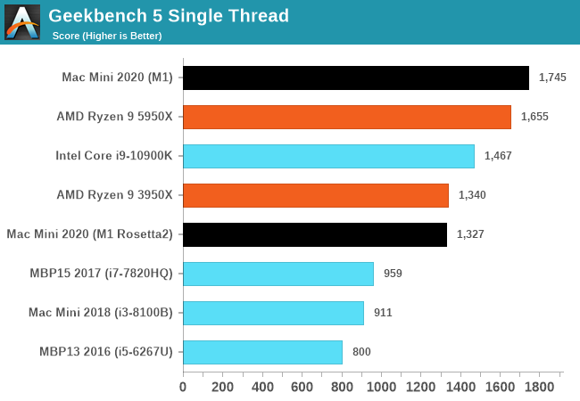
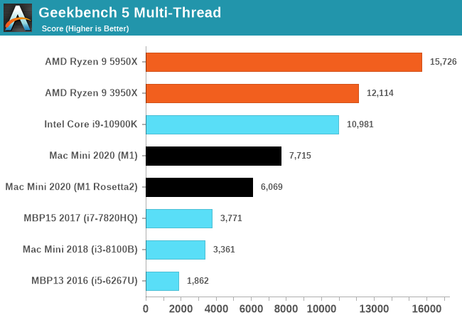
The performance of the new M1 in this “maximum performance” design with a small fan is outstandingly good. The M1 undisputedly outperforms the core performance of everything Intel has to offer, and battles it with AMD’s new Zen3, winning some, losing some. And in the mobile space in particular, there doesn’t seem to be an equivalent in either ST or MT performance – at least within the same power budgets.
What’s really important for the general public and Apple’s success is the fact that the performance of the M1 doesn’t feel any different than if you were using a very high-end Intel or AMD CPU. Apple achieving this in-house with their own design is a paradigm shift, and in the future will allow them to achieve a certain level of software-hardware vertical integration that just hasn’t been seen before and isn’t achieved yet by anybody else.
The software side of things already look good on day 1 due to Apple’s Rosetta2. Whilst the software doesn’t offer the best the hardware can offer, with time, as developers migrate their applications to native Apple Silicon support, the ecosystem will flourish. And in the meantime, the M1 is fast enough that it can absorb the performance hit from Rosetta2 and still deliver solid performance for all but the most CPU-critical x86 applications.
For developers, the Apple Silicon Macs also represent the very first full-fledged Arm machines on the market that have few-to-no compromises. This is a massive boost not just for Apple, but for the larger Arm ecosystem and the growing Arm cloud-computing business.
Overall, Apple hit it out of the park with the M1.Ryzen R5 3700X / Noctua NH-D15 / B550 AORUS ELITE V2 / Cooler Master H500 Mesh / 16Gb DDR4 @ 3800mhz CL16 / Gigabyte RTX 2070 Super / Seasonic Focus GX 750W / Sabrent Q Rocket 2 TB / Crucial MX300 500Gb + Samsung 250Evo 500Gb / Edifier R1700BT
-
06-02-21, 10:22 #14Moderador
- Registo
- Feb 2013
- Local
- Santo Tirso
- Posts
- 12,672
- Likes (Dados)
- 30
- Likes (Recebidos)
- 208
- Avaliação
- 4 (100%)
- Mentioned
- 7 Post(s)
- Tagged
- 0 Thread(s)
A resposta da Intel, à ameaça do M1 da Aple: Slides de powerpoint


 Ryzen R5 3700X / Noctua NH-D15 / B550 AORUS ELITE V2 / Cooler Master H500 Mesh / 16Gb DDR4 @ 3800mhz CL16 / Gigabyte RTX 2070 Super / Seasonic Focus GX 750W / Sabrent Q Rocket 2 TB / Crucial MX300 500Gb + Samsung 250Evo 500Gb / Edifier R1700BT

 Responder com Citação


Informação da Thread
Users Browsing this Thread
Estão neste momento 1 users a ver esta thread. (0 membros e 1 visitantes)

Bookmarks